Types of Storages for Computing System-On-Chips
We are living in an age where we generate the same amount of data each year that has been generated since antiquity. Ever wondered how and where these peta /exa/zetta bytes of data are stored?
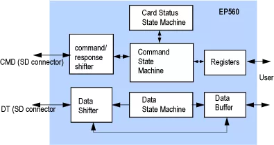
The SD Slave Controller is designed to reside within an SD memory, SDIO, or SD Combo Card.
The SD Slave Controller is designed to reside within an SD memory, SDIO, or SD Combo Card. It serves as an interface between the SD bus and user logic that provides the actual function of the card. It is designed to integrate with user logic to make various devices using the SD bus protocol, such as storage or wireless network card.
The SD slave controller supports both 1 and 4 bit SD interface (up to 8 bits in optional MMC support) and SPI mode. Data rate of up to 25Mbyte/sec (200Mbs) can be realized with SD interface. Features such as plug and play, auto-detection, error correction, write protection are standard with SD card interface and are supported.
As a slave device, the SD slave controller receives commands from the host through the SD interface. Most of the commands are processed locally by the controller without any help from the user logic. The majority of the standard SD register set is also implemented within the slave controller and process by the core without help from the user logic.
In case of memory or IO access that needs to be forwarded to the user logic, the slave controller handles all the SD bus protocol and presents the request to the user logic as simple read and write request through parallel address and data buses. Burst transfer of up to 2048 bytes per transfer and user defined wait states are supported on the user interface to maximize data bandwidth. The slave controller also contains data buffer to match the speed differences between the user interface and the SD interface. It allows a much more efficient use of the user interface.
SD Combo card and multi-function cards are supports by the EP560. With Combo card and multi-function, one user interface is dedicated for each function so all functions can operate in parallel.
With the EP560, SD card design can be realized with very little development cost. The designer can add SD memory and SDIO interface capability to the design by simply adding the EP560 module without changing the rest of the system architecture.
Note: some files may require an NDA depending on provider policy.

SDIO/SD Memory/MMC Slave Controller is a SD / eMMC Controller IP core from Eureka Technology, Inc. listed on Semi IP Hub.
Engineers should review the overview, key features, supported foundries and nodes, maturity, deliverables, and provider information before shortlisting this SD / eMMC Controller IP.
Yes. Buyers can compare this product with similar semiconductor IP cores or IP families based on category, provider, process options, and structured technical specifications.