Overview
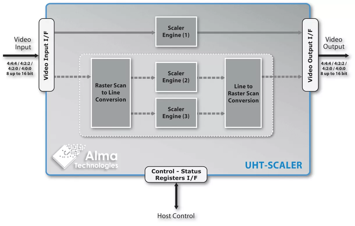
The UHT-SCALER core provides an image and video processing block which converts input images of one size and sampling format to output images of a different size and/or sampling format. It supports scaling of 4:4:4, 4:2:2, 4:2:0 and 4:0:0 (grayscale) image streams with 8- up to 16-bit color depth, using the BILINEAR, BICUBIC, LANCZOS and EXPFILTER scaling methods. The UHT-SCALER is a standalone and high-performance scaler core, designed for enabling high-quality and ultra-high throughput performance, even in low-end target silicon technologies. The UHT-SCALER is available for ASIC or AMD-Xilinx, Efinix, Intel, Lattice and Microchip FPGA and SoC based designs.
The core accepts the input image data in planar or interleaved scan order format and outputs the scaled image data in the same planar or interleaved format as the input.
The UHT-SCALER is very easy to use and integrate in a system. It requires minimal host intervention as it only needs to be programmed once per video sequence. Once programmed, it can scale an arbitrary number of video frames without the need of any further intervention or assistance by the host system CPU.
Learn more about Image Conversion IP core
Computer vision has made tremendous advances in the last several years due to the proliferation of AI technology. The intersection of big data and massive parallel computing changed the way in which machines are programmed to understand unstructured 2D and 3D data, such as video feeds from cameras.
Traditional IC design options that embedded system designers have had to choose from include fixed hardware devices such as standalone microprocessors, microcontrollers and ASSPs or configurable hardware devices such as FPGAs and cell-based ASICs. In this paper we present a new design option called Nextreme Structured ASICs which provide embedded system designers with a compelling alternative to custom embedded system design.
By Hantro
Configurable Processors for Video Processing SOCs
In this article, we show how fast video streams conforming to MIPI CSI2 rev2.0 over MIPI DPHY rev1.2 can be generated, using VLSI Plus’ SVTPlus-CSI2-F IP core, with simple off-FPGA analog front-end. The high bit rates can be achieved with a relatively slow FPGA clock frequency, trading off FPGA resources for simple timing closure.
Beyond pure process scaling which is necessary to meet today's price, power, and performance goals, chip designers have to grapple with tighter integration and product performance specialities in areas such as integrated power management, image sensing, application-specific data conversion, and enhanced display drivers.