RF SPDT Switch from 10-30 GHz used in TDD (Time Division Duplexing) mode for switching between TX and RX path with low loss, broadband and high isolation

Overview

RFSW01C RF SPDT Switch is used in TDD (Time Division Duplexing) mode for switching between TX and RX path with low loss, broadband and high isolation. This RF switch is Reflective type and the design incorporates series-shunt circuit elements with the locations optimized to achieve outstanding broadband performance in 10-30 GHz. The combination of broadband performance along with very fast switching and excellent settling time make this device ideal for many applications including Test & Measurement and broadband communication systems. This switch is designed using the 0.1um GaAs pHEMT process. Results are shown in datasheet with all parasitics & coupling effects at desired frequency.

Key Features

  • Broad band frequency Range: 10-30 GHz
  • Low Insertion Loss: 1.5 dB
  • High Isolation: 42.4 dB
  • Fast Switching Speed
  • Reflective Configuration
  • Ultra Low DC Power Consumption
  • Die size: 1.15 mm x 1.54 mm
  • This IP is similar in peformance with MACOM's MASW-011105

Benefits

  • Low insertion loss
  • High Isolation
  • Fast Switching Speed
  • Reflective Configuration
  • Ultra Low DC Power Consumption
  • Low cost
  • Porting: IP can be ported to 65nm Si / CMOS node

Block Diagram

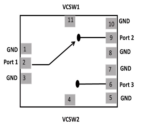
RF SPDT Switch from 10-30 GHz used in TDD (Time Division Duplexing) mode for switching between TX and RX path with low loss, broadband and high isolation Block Diagram

Applications

  • 5G mobile system
  • RF Antenna.
  • Military radios and Radar systems.
  • Space Based communication system.
  • EW and broadband communication systems.
  • Test & Measurement

Deliverables

  • Schematic and Net List
  • Abstract Model (.lib file)
  • Layout View (Optional)
  • Behavioral Model (Circuit & EM Simulation)
  • Extracted View (Optional)
  • GDSII
  • DRC, LVS, Antenna report
  • Test bench with saved configuration (Optional)

Technical Specifications

Foundry, Node
Win Semiconductor, 100 nm GaAs pHEMT process
Maturity
IC design and layout is complete, to be fabricated soon
Availability
Now
×
Semiconductor IP