PCIe 6.0 Retimer Controller with CXL Support
PCI Express® (PCIe®) 6.0 links operating at 64 GT/s using PAM4 signaling have a reach of up to 13 inches at nominal conditions on…
Overview
PCI Express® (PCIe®) 6.0 links operating at 64 GT/s using PAM4 signaling have a reach of up to 13 inches at nominal conditions on standard PCBs. Extending trace routing beyond this distance results in higher first bit error rates (FBER) and reduced link efficiency due to increased link recovery and retransmissions.
As new distributed architectures are deployed in data centers, greater flexibility is desired for chip placement including the need for longer trace lengths. Protocol-aware retimer chips can fully regenerate signals allowing board designers to extend reach and flexibly build various system topologies. The Rambus PCIe 6.0 Retimer Controller provides a complete digital data path solution that delivers best-in-class latency, power and area, and accelerates the time-to-market for PCIe 6.0 retimer chips.
How the PCIe 6.0 Retimer Controller Works
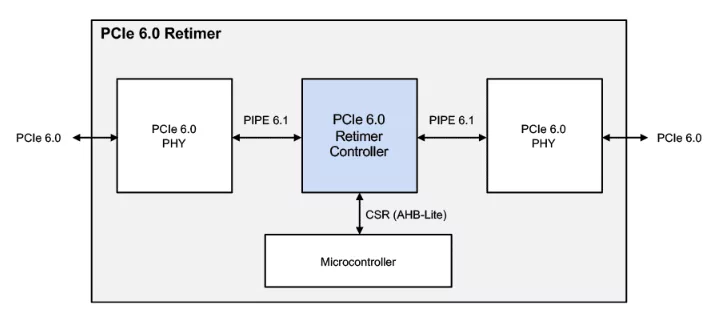
The PCIe 6.0 Retimer Controller provides a highly optimized low-latency data path for signal regeneration. It supports retimer chip PHYs via PIPE 5.2/6.1 interfaces. The control plane interface is provided via CSR (AHB-lite). The PCIe 6.0 Retimer Controller is CXL protocol aware and supports links using 64 GT/s and lower data rates of PCIe.
The PCIe 6.0 Retimer Controller provides designers with highly configurable equalization algorithms and adaptive behaviors. Its advanced RAS features enable control, observation and debugging of the controller and PHYs in silicon. Further, it supports various PCIe clocking architectures.
Key features
- Designed to the latest PCI Express 6.0 (64 GT/s), and capable of supporting 32.0, 16.0, 8.0, 5.0 and 2.5 GT/s link rates
- Supports x1, x2, x4, x8 and x16 link widths
- CXL aware and supports sync header bypass
- Supports PIPE 5.2/6.1 compatible PHYs
- Optimized data-path for low latency insertion
- Support for Figure of Merit and Up/Down PHY Equalization Feedback
- Highly configurable Equalization Algorithms with Adaptive Behaviors
- CSR (AHB-lite) control plane interface
- Advanced RAS features through pre-integrated XpressAgent debug monitor
- Supports SRIS, SRNS and common clock source modes
- Supports L0p power saving mode
Block Diagram

What’s Included?
- IP Files
- Verilog RTL source code
- IPXACT files for registers
- Software API in C & Python for
- XpressAgent (debug monitor)
- Documentation
- Retimer IP User Guide
- Getting Started Guide
- Reference Designs
- Synthesizable Verilog RTL source code
- Simulation environment and test scripts
- Synthesis project and DC constraintfiles (ASIC)
- Lint and CDC scripts
Files
Note: some files may require an NDA depending on provider policy.
Specifications
Identity
Provider

Learn more about CXL IP core
Cryptography Does Not Equal Security
Industry 1st CXL 4.0 Verification IP: Transforming AI and HPC Systems
Powering Up Efficiency: A Deep Dive into CXL L0p and its Verification
Demystifying CXL Memory Interleaving and HDM Decoder Configuration
From GPUs to Memory Pools: Why AI Needs Compute Express Link (CXL)
Frequently asked questions about CXL IP cores
What is PCIe 6.0 Retimer Controller with CXL Support?
PCIe 6.0 Retimer Controller with CXL Support is a CXL IP core from Rambus, Inc. listed on Semi IP Hub.
How should engineers evaluate this CXL?
Engineers should review the overview, key features, supported foundries and nodes, maturity, deliverables, and provider information before shortlisting this CXL IP.
Can this semiconductor IP be compared with similar products?
Yes. Buyers can compare this product with similar semiconductor IP cores or IP families based on category, provider, process options, and structured technical specifications.