Non-Power-of-Two FFT

Overview

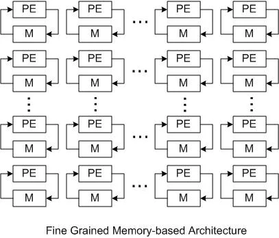
The transform computation is based on a new matrix formulation of the discreet Fourier transform1 (DFT) which decomposes it into structured sets of b-point DFTs. This avoids the inherent irregularities of the usual signal flow graph approach which typically requires complex commutators or permutation circuits, variable memory blocks, large butterfly units, global interconnections, and stage-to-stage differences, all of which degrade performance and require extra logic resources. Centar’s approach uses a small, regular, locally connected array, that keeps interconnect delays lower than cell delays, leading to high clock speeds/throughput and minimizes power. Because the circuit has a "memory based" architecture2, it is programmable so that a range of transform can be performed on the same array given adequate memory resources. (Data provided here applies to LTE SC-FDMA DFT transform size requirements). Finally, it includes a low overhead hybrid floating-point feature that increases dynamic range for a given fixed-point word size.

Key Features

  • Sample Rates: Very high clock speeds, e.g., as high as 450MHz in 65nm FPGA technology (highest commercially available FPGA-based throughputs)
  • FFT size: any size set of transforms (chosen at run-time) factorable into bases N=anbmcr…, where n,m,r are integers and the bases a,b,c,… are less than ~10. (Examples in this datasheet include the 35 transforms sizes required by LTE SC-FDMA)
  • Dynamic Range: combined block floating point and floating point architecture means smaller word lengths can be used for post-processing operations such as equalization (~6db/bit)
  • Scalability: array based architecture means arbitrarily higher throughputs are obtained by increasing array size
  • Power: array interconnects are entirely local, reducing parasitic routing capacitance to keep power dissipation low and clock speed high
  • Implementation FPGA: Centar's DFT circuit can be used in any FPGA fabric containing embedded multipliers and memories
  • Interface: simple

Benefits

  • Highest commercially available throughputs
  • Minimal use of LUT and register FPGA fabric
  • Programmability means circuit can be easily adapted to meet unique customer required functionality

Block Diagram

Non-Power-of-Two FFT Block Diagram

Applications

  • Applications specifically requiring non-power-of-two transform sizes, e.g., LTE Single Channel DFT Frequency Division Multiple Access (SC-FDMA) based protocols
  • Signal Processing (filtering, convolution, spectral analysis, data compression, filter banks)

Deliverables

  • Netlist (e.g., for Altera FPGAs a verilog *.qxp file for synthesis or *.vo file for simulation)
  • Synthesis constraints (e.g., for Altera FPGA’s an *.sdc file)
  • Modelsim Testbench (*.vo file for DFT circuit plus verilog testbench control file) that reads data from input file and outputs transform data to output file. Also includes Matlab verification utilities
  • Quartus LTE SC-FDMA Example Testbench (35 DFT sizes, 12-points to 1296-points) that includes pin-outs for use with an Altera Stratix III FPGA board development kit with (1) on-chip input/output data memories and a *.qxp file for the DFT circuit, that performs user selected number of blocks for a single size DFT; or (2) on-chip input/output data memories, verilog control circuitry, and a *.qxp file for the DFT circuit that cycles continuously through 2 blocks each of the LTE 35 different DFT sizes or (3) modelsim simulation environment of (2) using *.vo file.
  • Matlab behaviorial bit-accurate model (p-code) for specified DFT sizes
  • Documentation for above

Technical Specifications

Maturity
Hardware verified
Availability
Now
×
Semiconductor IP