LPDDR5X/5/4X/4 combo PHY at Samsung SF5A
OPENEDGES, the memory system IP provider, including DDR memory controller, DDR PHY, on-chip interconnect, and NPU IP together as …
Overview
OPENEDGES, the memory system IP provider, including DDR memory controller, DDR PHY, on-chip interconnect, and NPU IP together as an integrated solution or independent IP. They are tightly combined to bring synergy for high performance and low latency. OPENEDGES' integrated IP solutions are market and silicon-proven, featuring advanced architectures and proprietary technologies that enable customers to shorten their design and verification processes.
The LPDDR5X/5/4X/4 Combo OPHY features a state-of-art mixed-signal architecture that addresses the challenges of DRAM integration in high-performance and low-power environments. This architecture enables LPDDR5/4 Combo OPHY to overcome issues with long-term impedance drift and clock phase drift, allowing impedance and clock phase updates without interruption of data traffic. The programmable timing at the OPHY boundary combines flexibility with analog precision, resulting in low read/write latency between OMC and the LPDDR5X/5/4X/4 DRAM without sacrificing performance.
The LPDDR5X/5/4X/4 Combo OPHY was designed with subsystem and system-level considerations in mind. Built-in power management logic and advanced PLL design allow aggressive power state management and optimal system power usage.
At the system level, the LPDDR54 Combo OPHY was designed to minimize package substrate layer and PCB layer requirements, enabling usage in cost-sensitive applications and application processors.
Key features
- Compliant for JEDEC standards for LPDDR5X/5/4X/4 with PHY standards
- DFI 5.1 specification PHY Interface Compliant
- Support up to 4 ranks
- x16 and x32 channel support
- Multiple frequency states
- DQ Vref training supported
- PHY independent training and DRAM initialization
- Firmware (FW) based training
- Proprietary microcontroller with custom ISA
- Multiple DFICLK: CK ratios and DFICLK:CK: WCK ratio
- Tx and Rx channel equalization
- Voltage and temperature tracking of timing and impedance control circuit
- Flexible floor planning/bump mapping
- Transmitter and Receiver channel equalization
- Multiple low power saving states with IO retention
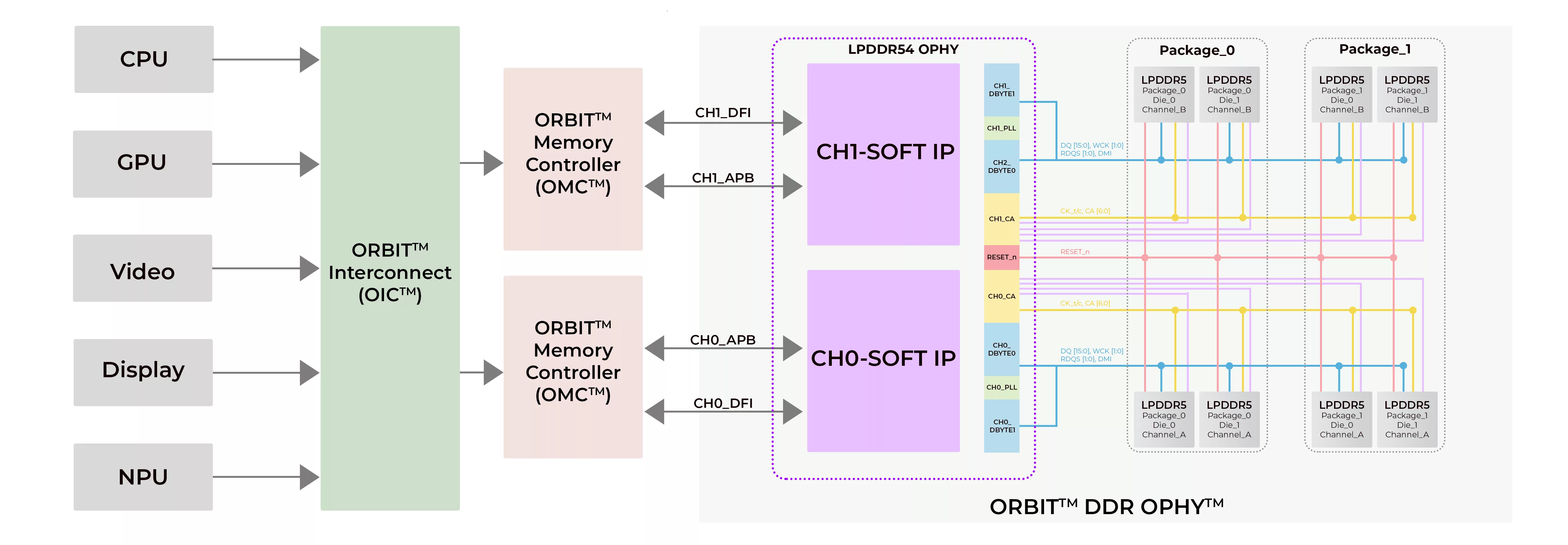
Block Diagram

Benefits
- Unbeatable performance-driven and low-power-driven PPA
- Ultra-low read/write latency with programmable PHY boundary timing
- Channel equalization with FFE and DFE
- Voltage and temperature drift compensation to maintain optimal data eye
- Firmware-based PHY independent initialization of DRAM and training
- Multiple frequencies state FSP with a fast switching time
- Multiple voltage domains for optimal voltage vs. frequency tuning
- Support low-cost package substrate and PCB
Applications
- Consumer edge devices
- Digital set-top-boxes
- TVs
- SSD controllers
- Application processors
What’s Included?
- Hard & Soft IP
- GDSII, LEF, LVS, timing models, etc.
- Verilog behavior models and encrypted RTL
- Synthesis and STA constraints
- Example test benches
- Documentation
- PHY Technical Reference Manual
- Implementation, package, and PCB design guidelines
- Test and characterization guidelines
- Physical verification reports
Files
Note: some files may require an NDA depending on provider policy.
Silicon Options
| Foundry | Node | Process | Maturity |
|---|---|---|---|
| Samsung | 5nm | SF5 | — |
Specifications
Identity
Provider

Learn more about LPDDR IP core
LPDDR flash: A memory optimized for automotive systems
A New Generation of LPDDR
Enabling Memory Choice for Modern AI Systems: Tenstorrent and Rambus Deliver Flexible, Power-Efficient Solutions
SOCAMM: Modernizing Data Center Memory with LPDDR6/5X
On-Device AI Semiconductors & High-speed Interconnects in the Physical AI era
Frequently asked questions about LPDDR IP
What is LPDDR5X/5/4X/4 combo PHY at Samsung SF5A?
LPDDR5X/5/4X/4 combo PHY at Samsung SF5A is a LPDDR IP core from OPENEDGES Technology, Inc. listed on Semi IP Hub. It is listed with support for samsung.
How should engineers evaluate this LPDDR?
Engineers should review the overview, key features, supported foundries and nodes, maturity, deliverables, and provider information before shortlisting this LPDDR IP.
Can this semiconductor IP be compared with similar products?
Yes. Buyers can compare this product with similar semiconductor IP cores or IP families based on category, provider, process options, and structured technical specifications.