LPDDR5X/5/4X/4 combo PHY at 7nm
OPENEDGES, the memory system IP provider, including DDR memory controller, DDR PHY, on-chip interconnect, and NPU IP together as …
Overview
OPENEDGES, the memory system IP provider, including DDR memory controller, DDR PHY, on-chip interconnect, and NPU IP together as an integrated solution or independent IP. They are tightly combined to bring synergy for high performance and low latency. OPENEDGES' integrated IP solutions are market and silicon-proven, featuring advanced architectures and proprietary technologies that enable customers to shorten their design and verification processes.
The LPDDR5X/5/4X/4 Combo OPHY introduces support for LPDDR5X speed bins and beyond, on top of the previously supported LPDDR5, 4X, 4 operating modes and speed bins. As with its predecessors, the 7nm LPLDDR5X/5/4X/4 OPHY test chip was brought up quickly in the lab and has achieved 8533 Mbps operation, the current maximum data rate for LPDDR5X, with dual-rank DRAM. The LPDDR5X OPHY will demonstrate quad-rank support in the near future. Also, it integrates key enhancements to its unique architecture, designed to enable maximum performance and flexibility while maintaining a footprint that is highly competitive to alternative LPDDR PHY solutions. In addition to the introduction of LPDDR5X support up to 8533 Mbps, the available configuration has been expanded to both 1x16 and 1x32, verified and ready for customer integration.
Supported Standards:
- JESD209-5A Low Power Double Data Rate 5 (LPDDR5)
- JESD209-5B Low Power Double Data Rate 5 (LPDDR5X)
- JESD209-4D Low Power Double Data Rate 4 (LPDDR4)
- JESD209-4-1 Low Power Double Data Rate 4X (LPDDR4X)
Key features
- Compliant with JEDEC JESD209-5B for LPDDR5X/5/4X/4 with PHY standards
- Delivering up to 8533Mbps
- DFI 5.1 specification PHY Interface Compliant
- Support up to 4 ranks
- Multiple frequency states
- DQ Vref training supported
- PHY independent training and DRAM initialization
- Firmware (FW) based training
- Proprietary microcontroller with custom ISA
- DFI Frequency ratio (CFI: CK ratio) 1:1
- Supports multiple frequency states
- Tx and Rx channel equalization
- Voltage and temperature tracking of timing and impedance control circuit
- Flexible floor planning/bump mapping
- Transmitter and Receiver channel equalization
- Multiple low power saving states with IO retention
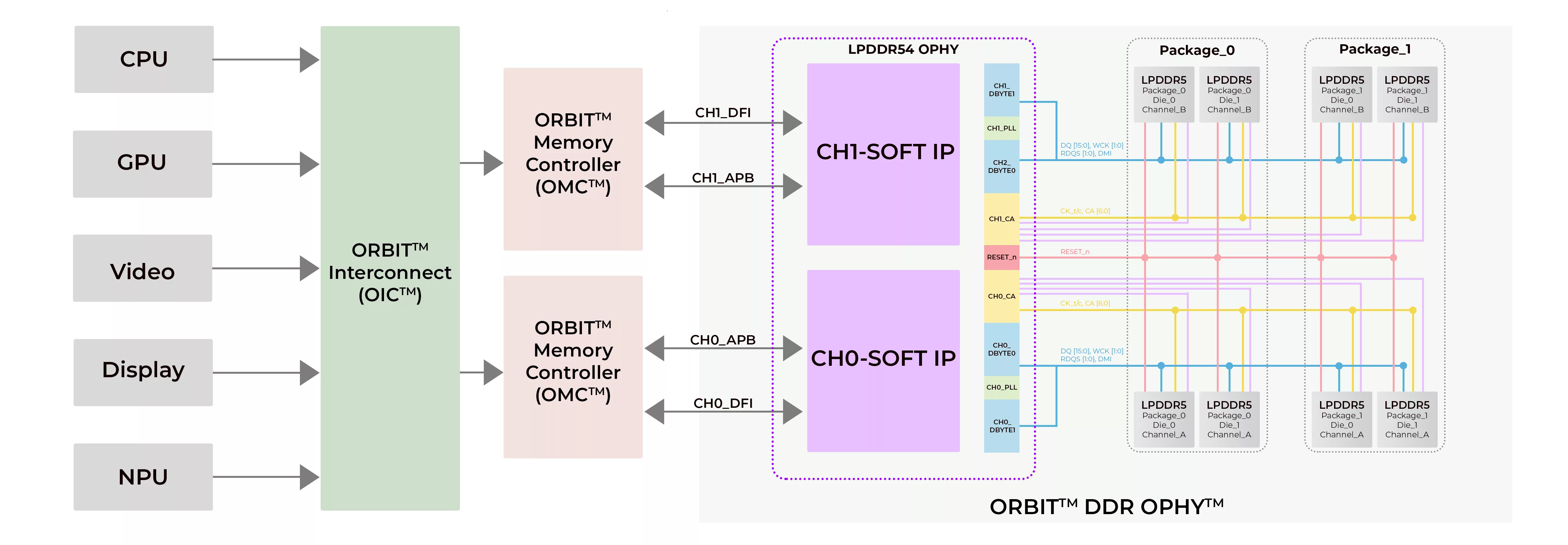
Block Diagram

Benefits
- Unbeatable performance-driven and low-power-driven PPA
- Ultra-low read/write latency with programmable PHY boundary timing
- Channel equalization with FFE and DFE
- Voltage and temperature drift compensation to maintain optimal data eye
- Firmware-based PHY independent initialization of DRAM and training
- Multiple frequencies state FSP with fast switching time
- Multiple voltage domains for optimal voltage vs. frequency tuning
- Support low-cost package substrate and PCB
Applications
- Consumer edge devices
- Digital set-top-boxes
- TVs
- SSD controllers
- Application processors
What’s Included?
- Hard & Soft IP
- GDSII, LEF, LVS, timing models, etc.
- Verilog behavior models and encrypted RTL
- Synthesis and STA constraints
- Example test benches
- Documentation
- PHY Technical Reference Manual
- Implementation, package, and PCB design guidelines
- Test and characterization guidelines
- Physical verification reports
Files
Note: some files may require an NDA depending on provider policy.
Specifications
Identity
Provider

Learn more about LPDDR IP core
LPDDR flash: A memory optimized for automotive systems
A New Generation of LPDDR
Enabling Memory Choice for Modern AI Systems: Tenstorrent and Rambus Deliver Flexible, Power-Efficient Solutions
SOCAMM: Modernizing Data Center Memory with LPDDR6/5X
On-Device AI Semiconductors & High-speed Interconnects in the Physical AI era
Frequently asked questions about LPDDR IP
What is LPDDR5X/5/4X/4 combo PHY at 7nm?
LPDDR5X/5/4X/4 combo PHY at 7nm is a LPDDR IP core from OPENEDGES Technology, Inc. listed on Semi IP Hub.
How should engineers evaluate this LPDDR?
Engineers should review the overview, key features, supported foundries and nodes, maturity, deliverables, and provider information before shortlisting this LPDDR IP.
Can this semiconductor IP be compared with similar products?
Yes. Buyers can compare this product with similar semiconductor IP cores or IP families based on category, provider, process options, and structured technical specifications.