Infiniband 4X Link Protocol Engine
The Link Protocol Engine (LPE) is single core solution incorporating in Link Layer of Open System Interconnect (OSI) which signif…
Overview
The Link Protocol Engine (LPE) is single core solution incorporating in Link Layer of Open System Interconnect (OSI) which significantly reduces the time and cost of implementing complex InfiniBand target system designs.
InfiniBand is an open architecture interconnect solution to handle and resolve bottleneck of multiple I/O streams simultaneously. Silicon Cores proven Intellectual Property expertise for various Link Layer and experience in high - speed channel interconnect.
The SI19IB40 is a switch - based serial I/O interconnect architecture operating at a speed of 10 Gbps for 4X in each direction. The SI19IB40 transmits and receives all kind of InfiniBand packets and generates and inspects the 32 bit Invariant Cyclic Redundancy Check (ICRC) and 16 bit Variant Cyclic Redundancy Check (VCRC).
The SI19IB40 is capable of supporting unicast as well as multicast addressing. The Maximum Transfer Unit supported by the SI19IB40 is 4096 Bytes. It has four data VLs and one management VL. The flow control mechanism implemented in the SI19IB40 is separate for each data VL and it is not implemented for the management VL.
Product Specifications :
- Fully synthesizable Register Transfer Level (RTL) Verilog HDL core.
- Test Bench Environment Verilog.
- Targeted FPGA Xilinx Spartan-6 / Virtex-6.
- Clock Frequency : 62.5 MHz.
Product Options :
- Adaptations : 32 bit PCI or AMBA Host Interface Possible.
- Add - ons : External Link - Phy Interface Possible (for 1X / 4X).
Key features
- Fully compliant Infiniband architecture based on Infiniband Trade Association (IBTA) 1.0.a Specifications.
- Compliance to Test Suites as provided by University of New Hampshire Inter - Operability Lab.
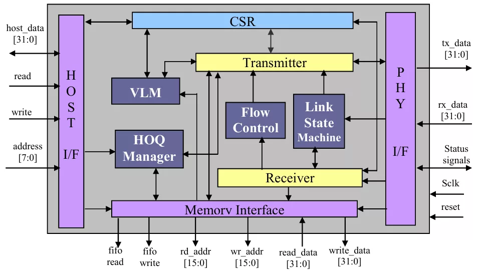
- Full Duplex Independent Transmit and Receive Data Path controlled by Link State Machine.
- Optimized for the use in Host and Target Channel Adapters.
- Supports all Management and Data Packets.
- Supports all Transport Services and Raw Packets.
- Four data Virtual Lanes (VL) plus Management Virtual Lane (MVL) support.
- Provides credit based Link level flow control to handle Pipelined data.
- Has a 4X (Single Link with Receive and Transmit) physical layer independent LINK - PHY Interface
- PHY Interface Data Rate for 4X is 8 GBPS LINK - PHY; 16 GBPS for Full - Duplex
- Distinct 32 bit data lines for transmit and receive.
- Supports max up to total 512 Kbytes of external buffer memory for transmit and receive.
- External Buffer memory can be fine tuned by user as per its need of application.
- Single clock domain throughout the system.
Block Diagram

Benefits
- Clock Frequency: 74.6MHz for FPGA (Standard: 62.5 MHz)
What’s Included?
- Fully synthesizable Register Transfer Level (RTL) Verilog HDL core.
- Test Bench Environment Verilog
Specifications
Identity
Files
Note: some files may require an NDA depending on provider policy.
Provider
Learn more about Infiniband IP core
cMPI: Using CXL Memory Sharing for MPI One-Sided and Two-Sided Inter-Node Communications
Ultra Ethernet's Design Principles and Architectural Innovations
UEC-LLR: The Future of Loss Recovery in Ethernet for AI and HPC
Designing the AI Factories: Unlocking Innovation with Intelligent IP
Growing demand for high-speed data in consumer devices gives rise to new generation of low-end FPGAs
Frequently asked questions about InfiniBand IP cores
What is Infiniband 4X Link Protocol Engine?
Infiniband 4X Link Protocol Engine is a Infiniband IP core from Silicon Cores - a Div. of Silicon Interfaces listed on Semi IP Hub.
How should engineers evaluate this Infiniband?
Engineers should review the overview, key features, supported foundries and nodes, maturity, deliverables, and provider information before shortlisting this Infiniband IP.
Can this semiconductor IP be compared with similar products?
Yes. Buyers can compare this product with similar semiconductor IP cores or IP families based on category, provider, process options, and structured technical specifications.