The Commsonic CMS0070 ISDB-S3 Modulator with integrated LDPC encoder has been designed specifically to address the requirements of the ARIB STD-B44 advanced wide-band digital satellite standard.
The core provides all the necessary processing steps to modulate a single transport stream (or baseband frame) into a complex I/Q signal for input to a pair of DACs, or an interpolating DAC device such as the AD9857(or AD9957). Optionally, the output can be selected as an IF to supply a signal DAC.
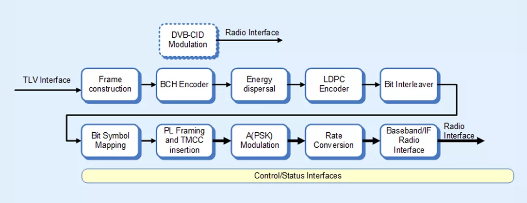
The active FEC code-rate and frame structure are automatically decoded from the TLV input stream. The design has been optimised to provide excellent performance in FPGA devices.
A description of the processing steps follows:
Frame construction. The ISDB-S3 slot and frame structure is formed using the information received over the TLV interface. Slot packet data and TMCC signalling information is sequenced through the encoding chain ready for final mapping and frame building.
Energy Dispersal. The energy dispersal block performs the ISDB-S3 scrambling randomisation polynomial.
BCH, LDPC Encoders. These blocks systematically encode each frame and apply error correction. Bit Interleaver, Mapping. The bit interleaver block applys block-based bit interleaving to the coded frame prior to symbol mapping.
PL Framing. This block constructs the physical layer framing around the encoded frame data together with the physical-layer frame and slot headers. The PL Framing block is also responsible for the insertion of the encoded TMCC signalling information.
A(PSK) Modulation. This block generates the complex constellation points from the mapped symbol data.
Rate Conversion. This block re-samples the complex samples output from the A(PSK) Modulation block at symbol-rate into complex samples at the core clock frequency.
Baseband-to-IF. This block provides the option to mix the signal up to a higher IF as defined by a software register. This block may be removed using synthesis options if it is not required.
Radio Interface. This block performs some final, register-selectable processing functions to optimise the output for the radio in the target application. For example, the data can be formatted to work with either twos-complement or offset-binary DAC devices. In addition the data is formatted to suit the external vice that could take separate I/Q, multiplexed I/Q or a single IF output.
Register Bank. The register bank provides a simple 32-bit interface for reading and writing registers within the modulator block. Full details of the registers within the modulator core are contained within the full data sheet.