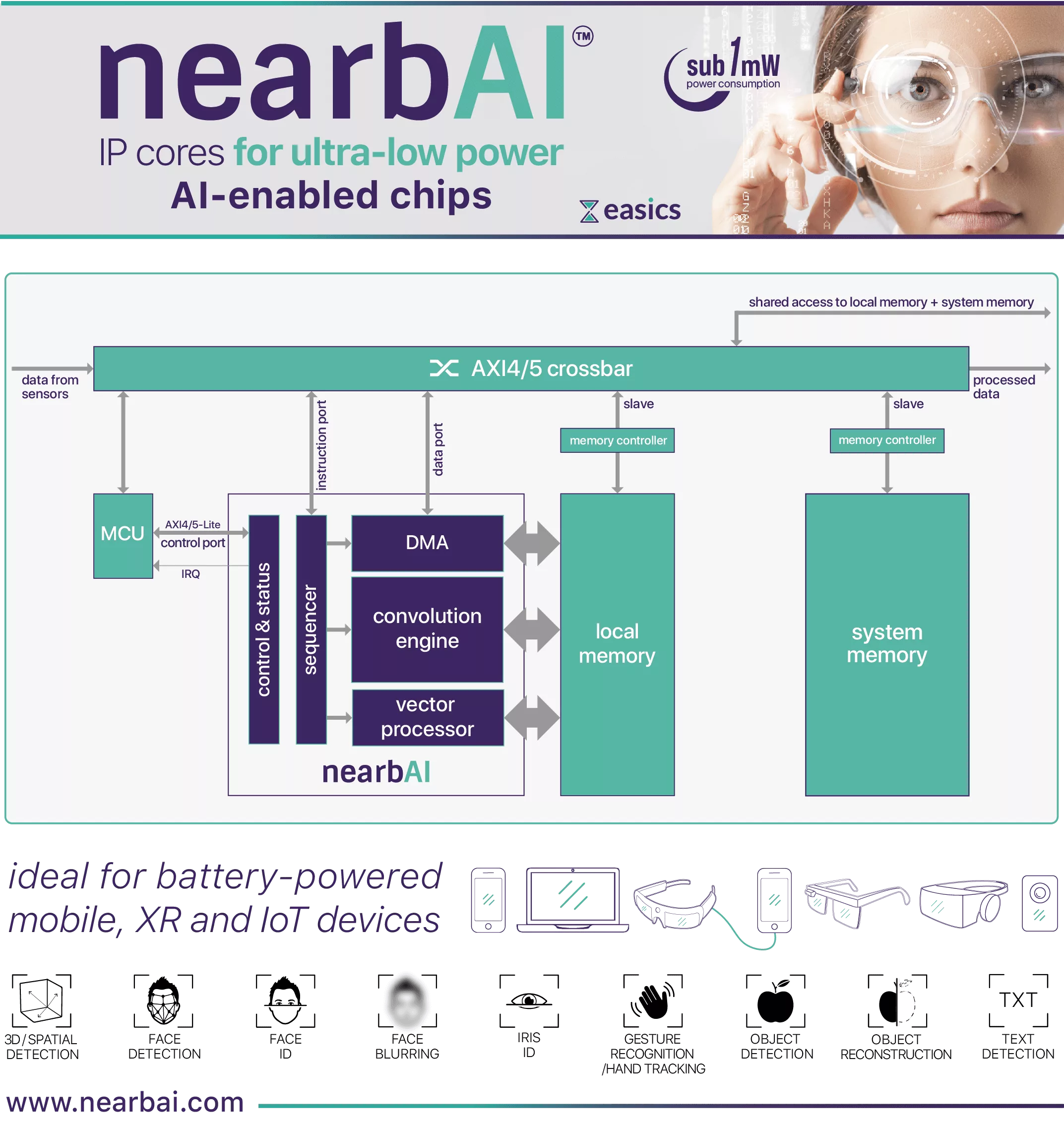
Overview
Each nearbAI core is an ultra-low power neural processing unit (NPU) and comes with an optimizer / neural network compiler. It provides immediate visual and spatial feedback based on sensory inputs, which is a necessity for live augmentation of the human senses.
- Optimized neural network inferencing for visual, spatial and other applications
- Unparallelled flexibility: customized & optimized for the customer’s use case
- Produces the most optimal NPU IP core for the customer’s use case: power, area, latency and memories trade-off
- Minimized development & integration time
Ideal for battery-powered mobile, XR and IoT devices
Why nearbAI?
Highly computationally efficient and flexible NPUs
- Enable lightweight devices with long battery life ... with ultra-low power, run heavily optimized AI-based functions locally
- Enable truly immersive experiences ... achieve sensors-to-displays latency within the response time of the human senses
- Enable smart and flexible capabilities ... fill the gap between “swiss-army knife” XR / AI mobile processor chips and limited-capability edge IoT / AI chips
Let's do a custom benchmark together:
provide us with your use case:
• Quantized or unquantized NN model(s):
ONNX, TensorFlow (Lite), PyTorch, or Keras
• Constraints:
Average power & energy per inference, silicon area, latency, memories, frame rate, image resolution, foundry + technology node
Learn more about Edge AI Accelerator IP core
While lightweight architectures like MobileNetV2 employ Depthwise Separable Convolutions (DSC) to reduce computational complexity, their multi-stage design introduces a critical performance bottleneck inherent to layer-by-layer execution: the high energy and latency cost of transferring intermediate feature maps to either large on-chip buffers or off-chip DRAM. To address this memory wall, this paper introduces a novel hardware accelerator architecture that utilizes a fused pixel-wise dataflow.
A look at Kinara’s accelerator and NXP processors which combine to deliver edge AI performance capable of delivering smart camera designs
In an ever-changing technology landscape, USB (Universal Serial Bus) has been a cornerstone since its inception in the mid-1990s. Initially designed to simplify the connection of peripherals to personal computers, USB has undergone significant transformations to meet the growing demands for faster data transfer rates, improved power delivery, and enhanced versatility.
Enter the Multi-Protocol SerDes (Serializer/Deserializer)—a flexible, reusable IP block that allows a single PHY to support multiple serial communication protocols, such as PCIe, SATA, Ethernet, USB, and more. This approach enables SoC vendors to meet diverse customer requirements and application needs without redesigning I/O for each target market.
Kurt Shuler, Arteris
William Ruby, Synopsys