Overview
The HBM2E memory controller IP is designed for use in applications requiring high memory throughput including performance-intensive applications in AI, HPC and graphics.
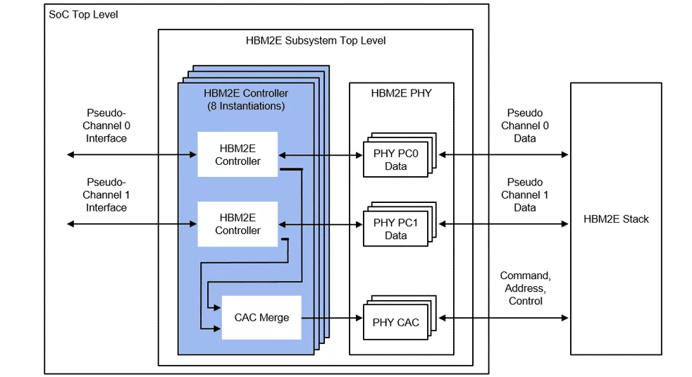
The HBM2E Interface Subsystem
HBM2E is a high-performance memory that features reduced power consumption and a small form factor. It combines a 2.5D/3D architecture with a 1024-bit wide interface operating at a lower clock speed (as compared to GDDR6) to deliver higher overall throughput at a higher bandwidth-per-watt efficiency for AI/ML and HPC applications.
The HBM2E controller supports both HBM2 and HBM2E devices with data rates of up to 3.6 Gbps per data pin. It supports all standard channel densities including 4, 6, 8, 12, 16 and 24 Gb. The controller maximizes memory bandwidth and minimizes latency via Look-Ahead command processing. The core is DFI compatible (with extensions added for HBM2E) and supports AXI or native interface to user logic.
The HBM2E controller is fully compliant with the JEDEC HBM2E JESD235 standard. It supports data rates up to 3.6 Gbps per data pin. The interface features 8 independent channels, each containing 128 bits for a total data width of 1024 bits. The resulting bandwidth is 461 GB/s per HBM2E memory device containing 2, 4, 8 or 12 3D-stacked DRAM.
The HBM2E controller together with the customer’s choice of PHY comprise a complete HBM2E memory interface subsystem.
Learn more about HBM IP core
As AI workloads continue to diversify, the systems that support them are evolving just as quickly. AI is no longer confined to the hyperscale data center. It is moving to the factory floor, into vehicles, and increasingly to the edge, where power, cost, and form factor constraints can matter just as much as raw performance.
With 3D stacking, high bandwidth and capacity can be achieved in a small, power-efficient footprint.
LLM inference is increasingly memory-bound, and HBM cost per GB now dominates system cost. Today’s HBM stacks include short on-die ECC, which tightens binning, raises price, and locks reliability policy inside the device. This paper asks a simple question: can we tolerate a much higher raw HBM bit error rate (BER) and still keep end-to-end correctness and throughput, without changing the HBM PHY or the fixed 32B transaction size?
HBM4 is the latest generation of the High Bandwidth Memory (HBM) that has become analogous to the Artificial Intelligence (AI) boom that is everywhere in today’s world. HBM is also increasingly being used in other applications like Data centers, autonomous driving systems, servers, cloud computing just to mention few domains where bandwidth and performance in a key requirement.
High-Bandwidth Memory (HBM) delivers exceptional bandwidth and energy efficiency for AI workloads, but its high cost per bit, driven in part by stringent on-die reliability requirements, poses a growing barrier to scalable deployment. This work explores a systemlevel approach to cost reduction by eliminating on-die ECC and shifting all fault management to the memory controller.
As artificial intelligence (AI) reshapes industries and advances technological frontiers, its success hinges on advanced memory capabilities. Leading this transformation is High Bandwidth Memory (HBM), which offers unparalleled speeds and efficiencies.