Fixed-size streaming FFT

Overview

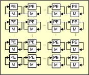
This FFT circuit employs unique architectural characteristics, different than any other FFT implementation. In particular the locality, simplicity and regularity of the processing core keeps interconnect delays lower than cell delays, leading to clock speeds that can approach the FPGA fabric limitations, e.g., "worst case" Fmax speeds >500MHz in 65nm FPGA technology. Short critical path lengths also lower power dissipation. Additionally, a novel "base-4" algorithm reduces the number of cycles needed per FFT to less than the transform size. Finally, it includes a low overhead hybrid floating-point feature that increases dynamic range for a given fixed-point word size.

Key Features

  • High Throughput: obtained from high clock rates (>500MHz using 65nm technology) and novel algorithms
  • FFT size: Any size power-of-two or non-power-of-two
  • Dynamic Range: combined block floating point and floating point architecture means smaller word lengths can be used for post processing operations such as equalization (~6db/bit).
  • Scalability: array based architecture means higher throughputs are obtained by increasing array size
  • Power: array interconnects are entirely local, reducing parasitic routing capacitance to keep power dissipation low and clock speed high
  • Implementation FPGA: Centar's DFT circuit can be used in any FPGA fabric containing embedded multipliers and memories.
  • Data I/O: Streaming, normal order I/O with fixed-point input words and output words consisting of a mantissa plus an exponent. (A normalized, fixed-point output can chosen as well).

Benefits

  • Easily modified to meet application requirements
  • Non-power-of-two options
  • Fastest commercially available throughputs

Block Diagram

Fixed-size streaming FFT Block Diagram

Applications

  • wireless communications and broadcast protocols, LTE, WiMax, radar, advanced noise cancellation, signal processing

Deliverables

  • Netlist (e.g., for Altera FPGAs a verilog *.qxp file for synthesis or *.vo file for simulation)
  • Synthesis constraints (e.g., for Altera FPGA’s an *.sdc file)
  • Modelsim Testbench (*.vo file for DFT circuit plus verilog testbench for control). Also includes Matlab verification utilities
  • Altera Stratix III FPGA board development kit testbench
  • Matlab behaviorial bit-accurate model (p-code) for LTE FFT transform sizes
  • Documentation for above

Technical Specifications

Maturity
Hardware verified
Availability
Now
×
Semiconductor IP