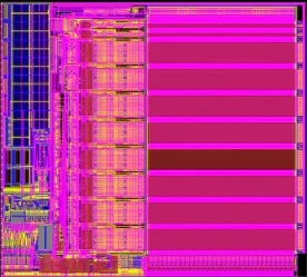
Embedded flash IP, 1.5V/5V 130BCD Plus
LEE Flash G1 (G1) is based on simple SONOS architecture and capable to scale down to 40nm geometry and supports auto grade temper…
Overview
LEE Flash G1 (G1) is based on simple SONOS architecture and capable to scale down to 40nm geometry and supports auto grade temperature and quality.
G1 is cost effective Flash solution up for medium memory capacity requirement up to several 100KBytes.
G1 also allows user to re-use IPs and Macros developed for standard CMOS platform because the adoption of G1 process module does not change characteristics of the logic transistors and SPICE model.
Key features
- Supports high temperature and long retention life time for severe automotive requirement
- Low power in Program/Erase operation for power critical applications
- Requires few (2~3) additional masks
- No change to SPICE model of Standard CMOS process, for re-using existing design and IP
- Short Test and Bake time to reduce chip cost
Block Diagram

What’s Included?
- Data Sheet
- Verilog
- Synopsys Model
- GDS
- Test Methodology
Files
Note: some files may require an NDA depending on provider policy.
Specifications
Identity
Provider

Learn more about Flash IP core
Concealable physical unclonable functions using vertical NAND flash memory
Flash Forward: MRAM and RRAM Bring Embedded Memory and Applications into the Future
Understanding the contenders for the Flash memory crown
Maximizing Performance & Reliability for Flash Applications with Synopsys xSPI Solution
LPDDR flash: A memory optimized for automotive systems
Frequently asked questions about Embedded Flash IP cores
What is Embedded flash IP, 1.5V/5V 130BCD Plus?
Embedded flash IP, 1.5V/5V 130BCD Plus is a Flash IP core from Floadia Corporation listed on Semi IP Hub.
How should engineers evaluate this Flash?
Engineers should review the overview, key features, supported foundries and nodes, maturity, deliverables, and provider information before shortlisting this Flash IP.
Can this semiconductor IP be compared with similar products?
Yes. Buyers can compare this product with similar semiconductor IP cores or IP families based on category, provider, process options, and structured technical specifications.