The CMS0010 DVB-S/-DSNG Modulator with integrated Reed-Solomon encoder has been designed specifically to address the requirements of the ETSI DVB-S forward-link satellite standard (EN 300 421), with further options available for compatibility with the ETSI DVB-DSNG digital satellite news gathering standard (EN 301 210).
The core provides all the necessary processing steps to modulate a single transport stream into a complex I/Q signal for input to a pair of DACs, or an interpolating DAC device such as the AD9857. Optionally, the output can be selected as an IF to supply a signal DAC.
The active FEC code-rate is controlled via a control register.
The design has been optimised to provide excellent performance in FPGA devices.
A description of the processing steps follows:
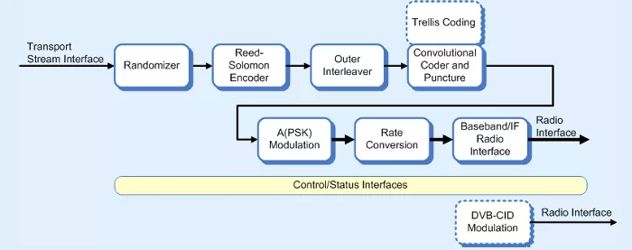
Randomiser. This block performs the energy dispersal and transport multiplex adaptation using the DVB randomisation polynomial 1+x14+x15 and also by inverting every eighth sync byte.
Reed-Solomon Encoder. This block generates Reed Solomon packets based on the DVB RS(204, 188) code with code generator polynomial:
g(x) = (x+λ0) (x+λ1) (x+λ2)… (x+λ15)
Where λ = 0x02, and field generator polynomial:
p(x) = x8 + x4 + x3 + x2 + 1
Outer Interleaver. This block performs the DVB outer interleaving function with depth I=12 as specified by the DVB standard.
Convolutional Encoder. This block performs the convolutional encoding as specified by DVB. Trellis Coding. This block performs the pragmatic trellis encoding as specified by DVB DSNG standard.
A(PSK) Modulation. This block generates the complex constellation points from the mapped symbol data.
Rate Conversion. This block re-samples the complex samples output from the A(PSK) Modulation block at symbol-rate into complex samples at the operating clock frequency. This provides an ultra flexible clocking strategy allowing the core to operate from low symbol-rates up to a maximum of twice the core clock frequency.
Baseband-to-IF. This block provides the option to mix the signal up to a higher IF as defined by a software register. This block may be removed using synthesis options if it is not required.
Radio Interface. This block performs some final, register-selectable processing functions to optimise the output for the radio in the target application. For example, the data can be formatted to work with either twos-complement or offset-binary DAC devices. In addition the data is formatted to suit the external vice that could take separate I/Q, multiplexed I/Q or a single IF output.
Register Bank. The register bank provides a simple 32-bit interface for reading and writing registers within the modulator block. Full details of the registers within the modulator core are contained within the full data sheet.