LVDS / sub-LVDS / DPHY TX - TSMC 6FFC
The LVDS/Sub-LVDS/DPHY Combo TX converts parallel RGB data and 7/8/10 bits of CMOS parallel data into serial data streams.
Overview
The LVDS/Sub-LVDS/DPHY Combo TX converts parallel RGB data and 7/8/10 bits of CMOS parallel data into serial data streams. A phase-locked clock is transmitted in parallel with the data streams over a dedicated high-speed link. The polarity of differential signals for each data lane can be controlled. The CL12661M10T2DM2FIP transmitter is an ideal means to solve EMI and cable size issues associated with high-speed CMOS interface.
* This IP is expandable to 4, 5, 8, 10 or more lanes.
* Porting is also possible for processes other than the target process.
* We can provide the original LINK controller (soft macro) that can be used with this PHY.
Key features
- Data Rate: Up to 1.0 Gbps for LVDS, subLVDS / 2.5Gbps for DPHY
- Clock polarity programmable
- Data polarity for each data lane is programmable
- Integrated Integer-N PLL
- 4 programable level of output differential voltage
- BIST function for loopback test
- Operational modes supported:
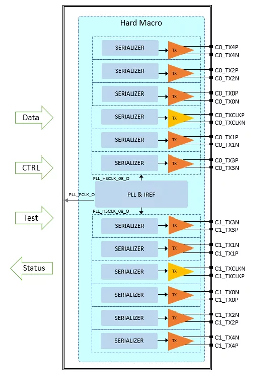
- to support LVDS dual link (5 data lanes + 1 clock lane) x 2 channel
- to support subLVDS link (5 data lanes + 1 clock lane) x 2 channel
- to support DPHY TX @ 2.5Gbps (4 data lanes + 1 clock lane)
Block Diagram

Benefits
- This IP has three operating modes and supports connection to a variety of displays.
- By developing an SOC equipped with this IP, customers can select the optimal interface from three interface types by changing the internal settings.
- This increases the flexibility of connected displays.
- In addition, LVDS mode allows amplitude adjustment when using long cables, increasing the flexibility of the connection environment.
- We can also supply link controllers that are compatible with this combo PHY.
- This IP can be implemented in a lane units and can be tailored to meet customer specifications.
Applications
- Display Application
- Automotive
- Navigation system
- DSC(Digital Still Camera)
What’s Included?
- Verilog Model (verilog / vcs)
- .db file / .lib(Option) file
- symbol / LVS netlist / Hspice netlist(Option)
- LEF, layer map file, layout technology file
- Layout Verification Report (DRC & LVS), Command file
- Datasheet
- Packaging and Layout Guideline / PCB Guideline
- Static Delay Analysis (STA) Guideline
- Testing Guideline (Option)
- RX Verilog Model and Test Vector(Option)
- Combo Link Layer IP(CD12661IP) and FPGA Board(Option)
Files
Note: some files may require an NDA depending on provider policy.
Silicon Options
| Foundry | Node | Process | Maturity |
|---|---|---|---|
| TSMC | 6nm | N6FF | Silicon Proven |
Specifications
Identity
Provider

Learn more about Single-Protocol PHY IP core
Design IP Faster: Introducing the C~ High-Level Language
Universal Flash Storage: Mobilize Your Data
Can MIPI and MDDI Co-Exist?
Enter the Inner Sanctum of RapidIO: Part 1
Networking software key to PICMG 2.16 optimization
Frequently asked questions about Single-Protocol PHY IP
What is LVDS / sub-LVDS / DPHY TX - TSMC 6FFC?
LVDS / sub-LVDS / DPHY TX - TSMC 6FFC is a Single-Protocol PHY IP core from Curious Corp. listed on Semi IP Hub. It is listed with support for tsmc Silicon Proven.
How should engineers evaluate this Single-Protocol PHY?
Engineers should review the overview, key features, supported foundries and nodes, maturity, deliverables, and provider information before shortlisting this Single-Protocol PHY IP.
Can this semiconductor IP be compared with similar products?
Yes. Buyers can compare this product with similar semiconductor IP cores or IP families based on category, provider, process options, and structured technical specifications.