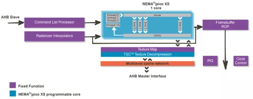
Innovation and architectural brilliance bring performance graphics rendering to the smallest and most power conscious embedded display devices. Minimal silicon area of only 0.11mm2 (@28nm), lowest MCU utilization of less than 5% and GPU power consumption of under 1mw, makes NEMA®|pico XS truly an agile GPU superstar.
2D Graphics Processor for Wearables/IoT
Overview
Key Features
- HARWARE COMPONENTS
- Programmable Shader engine with a VLIW instruction set
- Command list based DMAs to minimize CPU overhead
- Primitives Rasterizer
- Texture Mapping Unit
- Display Controller (optional)
- IMAGE TRANSFORMATION
- Texture mapping
- Point sampling
- Bilinear filtering
- Blit support
- Rotation any angle
- Mirroring
- Stretch (independently on x and y axis)
- Source and/or destination color keying
- Format conversions on the fly
- BLENDING SUPPORT
- Fully Programmable Alpha blending modes (source and destination)
- Source/Destination color keying
- DRAWING PRIMITIVES
- Pixel / Line drawing
- Filled rectangles
- Triangles (Gouraud Shaded)
- Quadrilateral
- TEXT RENDERING SUPPORTS
- Bitmap antialiased (A1 / A2 / A4 / A8 )
- Font Kerning
- Unicode (UTF8)
- COLOR FORMATS
- 32-bit RGBA8888 / BGRA8888 / ABGR8888
- 24-bit RGB
- 16-bit RGBA5551 / RGB565
- 8-bit ?8 / L8 / RGB332
- 4-bit A4 / L4
- 2-bit A2 / L2
- 1-bit A1 / L1
- TSCTM** (Optional) (Read Only)
- YUV Read Only
- ** Think Silicon Compression (proprietary)
Benefits
- Performance per mWatt per Dollar
- The NEMA®|GPU-Series performance per silicon area per clock frequency is unrivaled in its class. NEMA®|p has been designed to perform favorable against these critical performance benchmarks. As a result NEMA®|p uses 87% less active and 98% less idle power and has a 4 times smaller silicon footprint (compared to the competition), leading to significant cost reduction.
- Think Silicon's proprietary 4bpp (bits-per-pixel) real-time frame-buffer compression (TSCTMFB), the 6bpp texture compression and real-time de-compression (TSCTMT) benefits architects and finance controllers equally. The compressed images and the software libraries are so small in size that they fit into the internal SoC memory. As a result, expensive external DDR memory can be minimized or entirely eliminated. This reduces the SoC idle power consumption about impressive 98%, extends system battery life about 10 times and lowers the overall BOM cost. The combined performance and cost advantages make NEMA®|p to a Performance-Power-Cost leader in the class of 2D GPU's.
Block Diagram

Video
Nema|pico accelerating DirectFB - df_dok benchmark
Applications
- A fast 2D GUI interface and the NEMA®|pico XS is the perfect candidate to support entry level IoT-platforms, wearable and embedded devices with low cost and ultra-low power requirements supporting SoCs with a 32/64-bit MCU (e.g. ARM®| Cortex®| M processors) and provide fluid 2D graphics experience for a wide range of applications.
- Developers are able to create compelling 2D Graphical User Interfaces (GUIs) and software applications with ultra-long battery life at a significantly lower cost for power-memory-area constrained IoT devices.
Technical Specifications
Foundry, Node
synthesizable RTL
Maturity
silicon proven
Availability
now
Related IPs
- 2D Vector Graphics Accelerator / GPU (Graphics Processing Unit)
- High-performance 2D (sprite graphics) GPU IP combining high pixel processing capacity and minimum gate count.
- 2D (vector graphics) GPU IP Further advanced architecture for minimized CPU load and increased pixel performance in vector processing
- 2D (vector graphics) & 3D GPU IP A GPU IP combining 3D and 2D rendering features with high performance, low power consumption, and minimum CPU load
- 2D Graphics Hardware Accelerator (AXI4 Bus)
- High-performance and low-power 2D vector graphics IP core