Provider

NTLab is a vertically integrated microelectronics design center. It has 70+ experienced and qualified engineers.
NTLab specializes in the designing of mixed-signal and RF ICs and Systems-on-Chip. It has a wide range of own silicon-verified IP blocks: processor cores, interfaces, analog and high-frequency PHYs, etc., thus allowing customized design to be fast and predictable. In-company unique combination of competences in digital, analog and RF circuits and embedded software enables NTLab to participate in the projects that require deep research and utilize most sophisticated and advanced techniques: multi-system GPS/GLONASS/Galileo/BeiDou/NavIC(IRNSS)/QZSS/SBAS navigation, RF ID, wireless communications, etc. All designed ICs are provided with test and development tools, as well as with reference software.
NTLab offers a wide range of silicon proven analog/mixed-signal IPs in 0.35µm, 0.25 µm, 0.18 µm, 0.13 µm, 0.09 µm, 65nm, 55nm, 40nm, 28nm, 22 nm CMOS and SiGe BiCMOS processes. These IPs are suitable for devices targeted both consumer and industrial markets.
Most of these IPs have been proven in silicon on the foundries: Samsung, UMC, GlobalFoundries, SMIC, VIS, Tower, X-FAB, iHP, AMS, SilTerra, STMicroelectronics, Winfoundry.
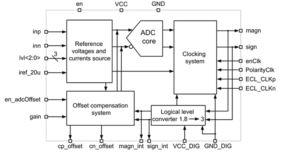
Learn more about ADC IP core
This paper introduces a novel closed-loop testing methodology for efficient linearity testing of high-resolution Successive Approximation Register (SAR) Analog-to-Digital Converters (ADCs). Existing test strategies, including histogram-based approaches, sine wave testing, and model-driven reconstruction, often rely on dense data acquisition followed by offline post-processing, which increases overall test time and complexity.
Analog to digital converters have three key input ports along with data output ports as per digital resolution requirements. These inputs ports are Analog Signal, Reference and Clock. If we compare across most of the converter architectures then clock frequency is directly related to output data rate and latency of the data conversion.
The growing availability of digital ICs like microcontrollers, microprocessors, and field-programmable gate arrays (FPGAs) allows developers to use complex digital processing techniques rather than analog signal conditioning. For this reason, analog-to-digital converters (ADCs) have become a widely-used component in mixed-signal circuits.
In high end RF systems, such as 5G radios, the requirements are so stringent that the source of this strongest unwanted tone can be the PLL. This article outlines how spurs in the input clock to the ADC or DAC may limit the SFDR. This in turn will set the requirements for the spurs for the input clock (from a PLL), in order to achieve a specific SFDR.
Power-sensitive applications such as Internet-of-Things (IoT) require a comprehensive power savings strategy within the system-on-chip (SoC). Techniques relying solely on the use of traditional power down modes and low supply voltage may not be enough to achieve the required power targets. The analog block is often assumed to be too sensitive and not compatible with aggressive power management techniques.
When continuously running a high speed ADC, it can be a challenge to deal with the firehose of raw data available at the output. To use City Semiconductor’s 2.5 GS/s 12-bit ADC, for example, 30 gigabits per second of data have to be accepted.