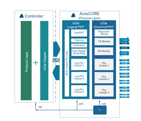
2-16Gbps Multi-Protocol IO Supporting BOW, OHBI and UCIe

Overview

AresCORE UCIe D2D PHY IP is the physical layer to enable Alphawave Semi’s Complete UCIe Solution for an open and robust chiplet ecosystem.

The AresCORE PHY IP is optimized for high-bandwidth density – Up to 36Gbps data-rate-per-lane, low-power, low-latency multi-module PHY and leverages silicon-proven analog IPs.

The AresCORE PHY IP can be configured to support advanced packaging such as Silicon Interposer, RDL Interposer, Integrated Fan-Out and Silicon Bridge for maximum density, and organic substrates for the most cost-effective solution covering all market segments.

The AresCORE PHY IP is available in leading-edge foundries across multiple technology nodes.

Key Features

  • The AresCORE UCIe D2D PHY IP provides
    •  High Tb/s of bandwidth per mm of shoreline, >11.8Tbps/mm (Advanced Package) and >2Tbps/mm (Standard Package)
    •  High data-rate-per-lane, up to 36Gbps
    • The AresCORE UCIe D2D PHY IP supports
    •  UCIe Standard Package (2D) with 16-bit and 32-bit modules
    •  UCIe Advanced Package (2.5D) with 32-bit and 64-bit modules
  • The AresCORE UCIe D2D PHY IP is an extremely power efficient, low-latency interconnect allowing the connection between two dies through short-reach low-loss channels. Our architecture allows SoC teams to reduce IO complexity and save power.
  •  Equipped with full calibrations, training, DFT, and reliability features
  •  Optimized for E/W and N/S implementations
  •  Delivered as a subsystem to support RDI or pre-integrated with streaming or PCIe/CXL controller
  •  Alphawave provides a platform for electrical, physical form factor, and protocol compliance
  •  Complete set of test vehicles for interoperability testing
  •  The AresCORE UCIe D2D PHY IP is compliant with IEEE 1149 boundary scan testing
  •  The Built-In Self-Test (BIST), internal and external loopback, and non-destructive eye diagram provide on-chip testability and visibility into channel performance
  •  Features for KGD (Known Good Die) testing

Benefits

  •  AI accelerators
  •  Server class CPUs
  •  Network switches designed for large compute
  •  FPGAs
  •  5G base stations
  •  IO and optical transceivers

Block Diagram

2-16Gbps Multi-Protocol IO Supporting BOW, OHBI and UCIe Block Diagram

Applications

  • AI accelerators
  • Server class CPUs
  • Network switches designed for large compute
  • FPGAs
  • 5G base stations
  • IO and optical transceivers

Technical Specifications

Foundry, Node
N5/N4p/N3e
Samsung
Pre-Silicon: 5nm
TSMC
Silicon Proven: 5nm , 6nm , 7nm
×
Semiconductor IP