multi-processor graphics IP
Filter
Compare
39
IP
from
17
vendors
(1
-
10)
-
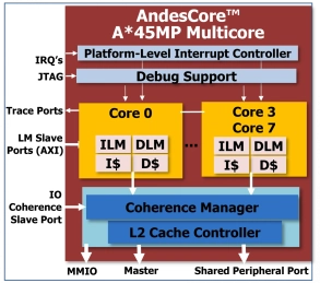
64-bit Multiprocessor with Level-2 Cache-Coherence
- 64-bit in-order dual-issue 8-stage pipeline CPU architecture
- Symmetric multiprocessing up to 8 cores
- Level-2 cache and cache coherence support
- AndeStar™ V5 Instruction Set Architecture (ISA)
-
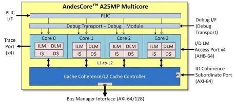
64-bit Multiprocessor with Level-2 Cache-Coherence
- Symmetric multiprocessing up to 4 cores
- Level-2 cache and cache coherence support
- AndeStar™ V5 Instruction Set Architecture (ISA). Compliant to RISC-V ISA IMACFDN, with Andes performance/functionality extensions
- Floating point extension

-
32-bit Multiprocessor with Level-2 Cache-Coherence
- AndesCore™ A25MP 32-bit multicore CPU IP is based on AndeStar™ V5 architecture.
- It supports RISC-V standard ‘IMAC-FD’ extensions, Andes contributed DSP/SIMD 'P' extension (draft), user-level interrupt 'N' extension, and Andes performance/functionality enhancements such as instructions for faster memory accesses, faster branch handling, and Andes Custom Extension™ (ACE) to add user defined instructions.
-
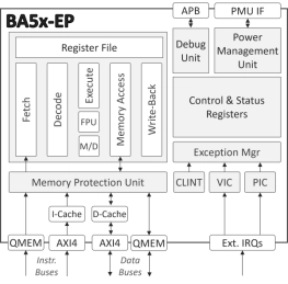
Enhanced-Processing Embedded RISC-V Processor
- The BA5x-EP is a highly-featured 32-bit RISC-V embedded processor IP core optimized for complex, processing-demanding applications.
- It is equipped with a floating-point unit and cache memories, supports hardware-level virtualization, and is suitable for concurrent execution in a multi-processor environment.
-
Vector-Capable Embedded RISC-V Processor
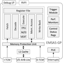
- The EMSA5-GP is a highly-featured 32-bit RISC-V embedded processor IP core optimized for processing-demanding applications.
- It is equipped with floating-point and vector-processing units, cache memories, and is suitable for concurrent execution in a multi-processor environment.
-
Compact Embedded RISC-V Processor
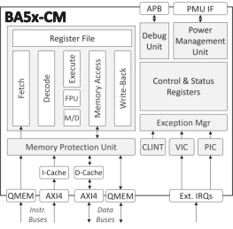
- The BA5x-CM is a feature-rich 32-bit deeply embedded processor.
- Equipped with a floating-point unit and an instruction cache memory and supporting concurrent execution in a multiprocessor environment, it is well-suited to a wide range of edge IoT and similar applications.
-
Simulation VIP for AMBA CHI-C2C
- Incorporating the latest protocol updates, the Cadence Verification IP for CHI-C2C provides a complete bus functional model (BFM), integrated automatic protocol checks, and a coverage model.
- Designed for easy integration in testbenches at IP, systems with multiple CPUs, accelerators, or other device chiplets, the VIP for CHI-C2C provides a highly capable compliance verification solution that supports simulation, formal analysis, and hardware acceleration platforms.

-
32-Bit & 64-Bit High Performance Processor - 9-Stage Pipeline, Dual-issue
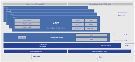
- 900 Series processors include four different classes: N900 (32 bit), U900 (32 bit + MMU), NX900 (64 bit) and UX900 (64 bit + MMU). With MMU, UX900 supports heavyload operating systems such as Linux. 900 Series can be applied to edge computing, data center, networking, etc.
-
RVA23, Multi-cluster, Hypervisor and Android
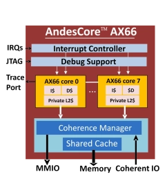
- 64-bit out-of-order 4 wide decode 13-stage CPU core with 128 reordering buffers and 8 functional pipelines
- Symmetric multiprocessing up to 8 cores
- Private L2 cache support
- Level-3 shared cache and coherence support
-
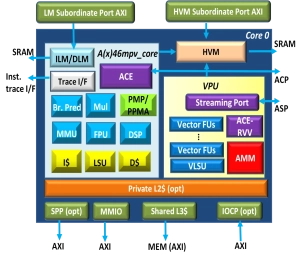
64 bit RISC-V Multicore Processor with 2048-bit VLEN and AMM
- 2 different packages with or without vector: AX46MPV, AX46MP
- in-order dual-issue 8-stage CPU core with up to 2048-bit VLEN
- Symmetric multiprocessing up to 16 cores
- Private Level-2 cache
- Shared L3 cache and coherence support
