PCIe Gen 3 IP
Filter
Compare
44
IP
from
19
vendors
(1
-
10)
-
AXI PCI Express (PCIe) Gen 3
- Maximum Payload Size (MPS) up to 256 Bytes
- Messaged Signaled Interrupt (MSI)
- Memory mapped AXI4 access to PCIe space
- PCIe access to memory mapped AXI4 space
-
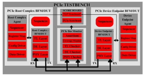
PCIe Gen 5 - Validates high-speed designs, ensuring compliance and error-free performance
- PCIe Gen 5 Verification IP offers a robust solution for validating designs based on the PCI Express 5.0 specification, delivering high-speed data transfer, protocol compliance, and advanced error injection. It ensures seamless integration into existing environments.
- The product supports a range of industries, optimizing high-performance computing, AI, storage solutions, and more. With applications in data centers, automotive, IoT, and gaming, PCIe Gen 5 enhances efficiency and scalability across diverse sectors
-
PCIe Gen 4 - Enables high-speed verification, error handling, and protocol compliance
- PCIe Gen 4 Verification IP ensures efficient, high-speed signaling, protocol conformance, error handling, and system interoperability for PCIe Gen 4 designs. It accelerates validation with automated testbenches, ensuring compliance and reducing time-to-market.
- PCIe Gen 4 Verification IP is essential for chip design, SoCs, servers, data centers, storage, GPUs, telecom equipment, and automotive electronics. It validates robust PCIe Gen 4 integration, ensuring performance, reliability, and interoperability

-
PCIe Gen 7 Verification IP
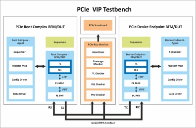
- The PCIe Gen 7 Verification IP provides an effective & efficient way to verify the components interfacing with PCIe Gen 7 interface of an IP or SoC.
- The PCIe Gen 7 VIP is fully compliant with latest PCI Express Gen 7 specifications. This VIP is a light weight with an easy plug-and-play interface so that there is no hit on the design cycle time.
-
PCIe Gen 6 controller IP
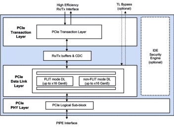
- Designed to the latest PCI Express 6.0 (64 GT/s), 5.0 (32 GT/s), 4.0 (16 GT/s), 3.1/3.0 (8 GT/s), and PIPE 6.x (8, 16, 32, 64 and 128-bit) specifications
- Supports SerDes Architecture PIPE 10b/20b/40b/80b width
- Supports original PIPE 8b/16b/32b/64b/128b width
-
PCIe Gen 6 Verification IP
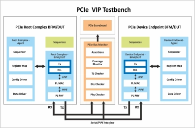
- Compliant with PCI Express Specifications 6.1 (64GT/s), 5.0 (32GT/s), 4.0 (16GT/s), 3.1 (8GT/s), 2.0 (5GT/s) and 1.1 (2.5GT/s).
- Support for 64.0 GT/s Data Rate per lane with backwards compatible.
- Support for new PAM4 Signalling and Gray Coding.
- Support for both Flit Mode & Non-Flit Mode.
-
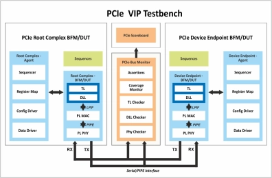
PCIe Gen 5 Verification IP
- Support for 32.0 GT/s Data Rate per lane with backwards compatible.
- Optimizing the Link to skip equalization at lower Data Rates when supporting 32.0 GT/s(optional feature).
- Lower pin count in pipe interface when supporting 32.0 GT/s.
- Support for newly added phy serdes architecture in pipe specification 5.0 .
-
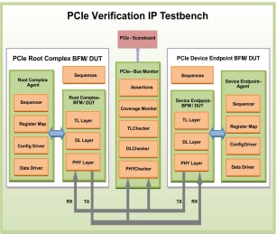
PCIe Gen 2 Verification IP
- Compliant with PCI Express Specifications 2.0 (5GT/s) and 1.1 (2.5GT/s).
- Verification IP configurable as PCI express Root Complex and Device Endpoint.
- Configurable LinkWidth: x1, x2, x4, x8, x12, x16, x32.
- Configurable pipe width : 8,16,32,64
-
PCIe 3.0 Serdes PHY IP, Silicon Proven in GF 22FDX
- Silicon Proven in GF 22GDX with 0.8V and 1.8V power supply.
- Compatible with PCIe base Specification
- Support 32-bit/16-bit parallel interface
- Support for PCIe3(8.0Gbps)

-
PCIe 3.1 Serdes PHY IP, Silicon Proven in TSMC 40LP
- Support PHY interface (PIPE4.3) enables multiple IP sources for USB3 MAC layer
- Supports 5.0Gbps and 10Gbps serial data transmission rate Supports 16-bit or 32-bit parallel interface Data and clock recovery from serial stream
- Support 8b/10b encoder/decoder(5Gbps), 128/130 encoder/decoder(BGbps) and error indication
- Tunable receiver detection to detect worse case cables