Memory Subsystem IP
Filter
Compare
205
IP
from
52
vendors
(1
-
10)
-
Functional-Safety & Secure LPDDR3 Memory Subsystem
- Safe & Secure-LPDDR3 that is ready for ASIL (Automotive Safety Integrity Level) and secure by design
- Functional Safety out-of-the box design, with an extensive ASIL documentation package.
- Integrated security features into the controller. Characterized for extended operating conditions and long-term reliability.
-
Hyper-Bandwidth Multichannel Memory Subsystem
- Hyper-Bandwidth Multi-Channel - The fastest, most observable LPDDR3 subsystem you can drop into an SoC
- Supports an aggressive bandwidth envelope for LPDDR3, JEDEC-2133Mbps and up to 3200 Mbps on select process nodes.
- Includes hard QoS enforcement, traffic shaping, performance observability & self-tuning PHY front-end.
-
Ultra-Low-Power LPDDR3/LPDDR2/DDR3L Combo Subsystem
- Ultra-low Power-Smallest, sleepiest LPDDR3 subsystem for real bandwidth & compatibility
- Power-first architecture optimized for low-speed & small footprint, with multiple system-level power saving features.
- Pin-compatible design enables seamless migration to next-gen devices and supports board-reuse.
-
Bluetooth Low Energy Subsystem IP – v6.0
- The SB1001-CM BLE 6.0 digital modem and baseband controller IP enables industry-leading, ultra-efficient, wireless SoCs for multiple connected applications.
- Industry leading modem link budget for RF environment reliability and resilience, industry leading support for scalable numbers of connections and a Zephyr driver for ease of host integration
-
Bluetooth Low Energy Subsystem IP
- The BLE v6.0 Subsystem IP consists of an integrated Controller and Modem paired to a proprietary RF on T22 ULL.
- It is ideally suited to ASIC developers or fabless semiconductor companies who want to add BLE functionality without the hassle of dealing with multiple IP vendors or design groups.
-
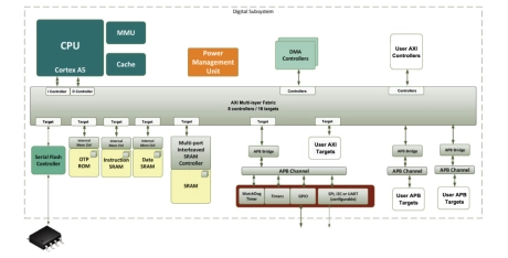
AXI Performance Subsystem - ARM Cortex A
- The AXI Performance Subsystem is an AMBA® AXI4 based system that is useful as the digital infrastructure for building SOCs needing high performance.
- This system contains an 8 Master component, 16 Slave component AXI4 multi-matrix for supporting multiple high speed user AXI Master components while providing high performance with Cortex-A5 class processors.
-
Data Movement Engine - Turnkey network compute subsystem for data movement applications.
- Industrial Networking: Rapid packet processing of data through multiple, switched ethernet ports with support for factory automation protocols
- 5G/6G Communications: Scalable L2/L3 Ethernet switch with flexible port counts/speeds, including TSN and security
- Automotive Gateway: High-speed data packet networking with multiple communication interfaces and support for switching and bridging
- Datacenter Infrastructure: Standalone data processing units to handle highly multiplexed data streams corresponding to millions of network connections with high efficiency and low power
-
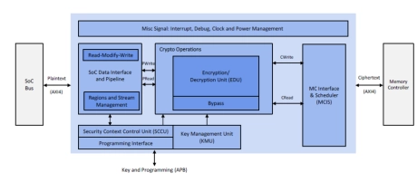
Inline memory encryption engine for ASIC SoCs
- 128/512-bit (16-byte) encryption and decryption per clock cycle throughput
- Bidirectional design including separate crypto channels for read and write requests, ensuring non-blocking Read
- Read-modify-write supporting narrow burst access.
- Zeroization and support for memory initialization
- Latency: <28 clock cycles for unloaded READ
-
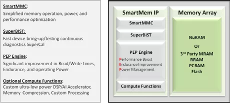
SmartMem Subsystem IP
- Fully synthesizable and configurable memory subsystem IP that enables significant improvement in power, performance and endurance not only for NuRAM but also other third party MRAMs as well as RRAM, PCRAM and Flash
-
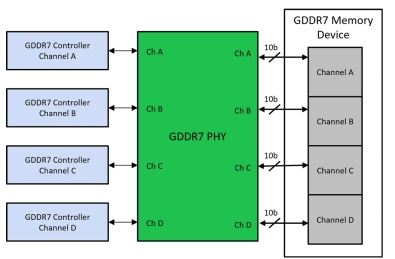
GDDR7 Memory Controller
- Supports up to 40 Gbps per pin operation
- 2.5 GHz CK4 clock
- 1.25 GHz controller clock
- Internal data path 32x memory width (i.e. 256 bits for 8-bit memory)
- Optimized for high efficiency and low latency across a wide range of traffic scenarios (random/sequential, short/long bursts, etc.)
- Optimized command sequence for highest bus utilization including per-bank refresh scheduling: single queue structure handles look-ahead activates/ precharges and read/write ordering for minimal latency