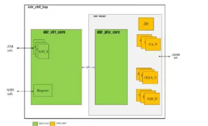
DDR3 SDRAM Controller IP
Filter
Compare
84
IP
from
14
vendors
(1
-
10)
-
DDR3 SDRAM Controller
- Support for all LatticeECP3 “EA” devices
- Interfaces to Industry Standard DDR3 SDRAM components and modules compliant with JESD79-3, DDR3 SDRAM Standard
- Interfaces to DDR3 SDRAM at speeds up to 400 MHz / 800 Mbps in -8 speed grade devices
- Supports memory data path widths of -8, -16, -24, -32, -40, -48, -56, -64 and -72 bits
-
DDR3 SDRAM Controller
- Supports industry standard Double Data Rate (DDR2 and DDR3) SDRAM.
- Pipeline access allows continuous data bursting and hidden command execution.
- Page hit detection supports fast column access and multiple open banks.
- High speed implementation with standard DFI support for hard DDR PHY.
-
Intel® FPGA IP for DDR3 SDRAM High-Performance Controller
- The Intel FPGA Intellectual Property (IP) for DDR3 SDRAM High-Performance Controller provides simplified interfaces to industry-standard DDR3 SDRAM devices and modules
- The Intel FPGA IP work in conjunction with the Intel FPGA ALTMEMPHY physical interface IP
- These DDR3 SDRAM IP functions offer a half-rate interface to the customer application logic.
-
DDR3 SDRAM Controller IP with advance feautures package
- Supports DDR3 protocol standard JESD79-3F Specification.
- Compliant with DFI-version 2.0 or higher Specification.
- Supports all the DDR3 commands as per the specs. Supports up to 16 AXI ports with data width upto 512 bits.
- Supports controllable outstanding transactions for AXI write and read channels
-
DDR3 SDRAM Memory Controller
- Supports DDR3 SDRAM memory devices on AMD-Xilinx 7 Series FPGAs
- Size optimized – ideal for low cost 7 Series FPGAs (Artix-7, Spartan-7)
-
DDR 4/3 Memory Controller IP - 2400MHz
- Support s DDR 4 /DDR3 SDRAM
- 16 bit s width , Single Channel DDR 4 /DDR3 SDRAM Interface .
- 16 bits for per channel, could support 2 x8 bits DDR3, but could not support 2 x8 bits DDR4.
- Memory Clock up to 6 66 MHz, DFI Clock up to 666 MHz .
-
High-Performance Memory Controller II SDRAM Intel® FPGA IP Core
- The High-Performance Memory Controller II SDRAM Intel FPGA IP core handles the complex aspects of using DDR, DDR2, and DDR3 SDRAM at speeds up to 933 MHz
- The intellectual property (IP) core initializes the memory devices, manages SDRAM banks, translates read-and-write requests from the local interface into all the necessary SDRAM command signals, and performs command and data reordering.

-
High Performance DDR 3/2 Memory Controller IP
- Supports DDR3/DDR2 SDRAM
- 16 bits width DDR2/DDR3 SDRAM Interface
- Memory Clock up to 462MHz, DFI Clock up to 462MHz
- Support DDR2 667/800/1066 and DDR3 667/800/1066/1333/1600/1866
-
DDR4 / DDR3/ DDR3L / LPDDR4 Memory Controller IP optimized for low latency
- Support DDR3 / DDR3L / DDR4/ 3DS DDR4/ LPDDR4 / MRAM
- Support x8/x16/x32 DRAM data bus configuration (programmable)
- Support Multi-Ranks DRAM configuration
- DDR base on DFI spec 4.0 compliant.