ONFI IP
Welcome to the ultimate ONFI IP hub! Explore our vast directory of ONFI IP cores
The ONFI IP cores are used to access the external NAND flash for high speed transactions of multiple pages of read or write data taking advantage of the pipeline performance of newer enterprise NAND flash devices.
All offers in
ONFI IP
Filter
Compare
51
ONFI IP
from
17
vendors
(1
-
10)
-
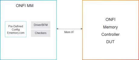
Simulation VIP for ONFi
- Hundreds of protocol and timing checkers to easily catch design bugs
- Hundreds of predefined configurations based on specific memory vendors' part numbers, datasheets, or generic JEDEC definitions available on ememory.com(opens in a new tab)
- Transaction and memory callbacks for all protocol, model states and device memory events
-
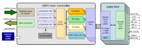
ONFI NAND PHY
- ONFI 1/2/3/4/5 compliant
- SLC/MLC/TLC support
- SDR (Asynchronous) mode 0 to 5
- NV-DDR (Source Synchronous) mode 0 to 5
- NV-DDR2 mode 0 to 10
-
3600 ONFI NV-DDR3 and NV-LPDDR4 with Optional DFE
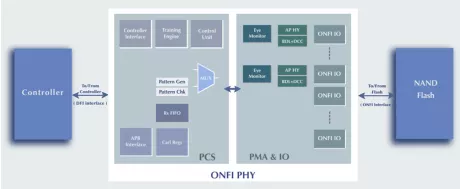
- Our 3600 ONFI PHY is a silicon proven complete IP solution, including I/O, PMA, PCS and test engine with optional one-tap DFE.
- The IPT 3600 ONFI PHY facilitates high-speed data transfer between NAND flash memory and host controllers.
- This interface is crucial for enhancing the performance and reliability of storage solutions in various applications, from consumer electronics to industrial systems.

-
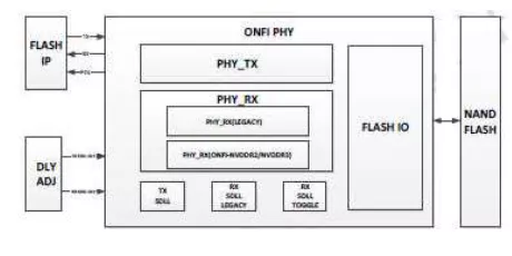
ONFi PHY 4.0 (FPHY+MDLL+SDLL Regulator) (Silicon Proven in TSMC 28HPC+)
- Support ONFi 4.0 IO Electrical Specification
- Support Legacy up to 50MHz
- Support NV-DDR2 with operating frequency up to 533Mbps
- Support NV-DDR3 with operating frequency up to 800Mbps
-
4800 ONFI NV-DDR3 and NV-LPDDR4 with 4-tap DFE
- Supports Both NV-DDR3 and NV-LPDDR4 with 4-tap DFEs
- Support Decision Feedback Equalization (DFE): For extra high loading, DFE can reduce errors and improve data integrity
- Compliant with JEDEC 6.0 (TBD) and JESD 230G specifications
- Supports real-time PVT data-eye monitoring
-
ONFI Nand Flash Software Driver
- Compliant with ONFI 3.2 and backward compatible to ONFI 3.0, 2.3 and 1.0
- Supports SDR, NV-DDR and NV-DDR2, Toggle DDR/DDR2 modes
- Easy-to-use interface for applications
- Support up to NAND with 16K page size

-
ONFI 5.0 NAND Fash PHY IP Compliant to JEDEC
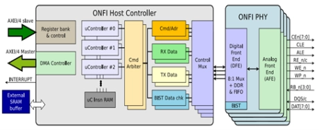
- The ONFI 5.0 PHY IP is designed to connect seamlessly with their ONFI 5.0 Host Controller IP.
- The ONFI 5.0 PHY has complete SDR, NV-DDR, NV-DDR2, NV-DDR3 and NV-LPDDR4 TX/RX functionality and supports all the speeds defined in the ONFI specification while remaining backwards compatible with the prior versions of the ONFI specifications.
-
ONFI 5.0 NAND Flash Controller IP Compliant to JEDEC
- The NAND flash controller IP provides easy, reliable access to an off-chip NAND flash. It supports all modes of the Open NAND Flash Interface (ONFI) Specification, revision 5.0, release candidate 0.5, dated 1 March 2021.
- It is backwards compatible, supporting the Single Data Rate (asynchronous) mode, the double data rate moves NV-DDR, NV-DDR2, and NVDDR3, to include the latest NV-LPDDR4 recently introduced in the latest revision.

-
ONFI 4.2 NAND Flash Software Driver
- The NAND Flash Controller IP Core is a full-featured, easy to use, synthesizable core, easily integrated into any SoC or FPGA development. Designed to support SLC, MLC and TLC flash memories, it is flexible in use and easy in implementation.
- The controller works with any suitable NAND Flash memory device up to 1024Gb from leading memory providers – Micron, Samsung, Toshiba and Hynix.

-
ONFI 4.2 NAND Flash Controller & PHY IP Compliant to JEDEC
- The NAND Flash Controller IP Core is a full-featured, easy to use, synthesizable core, easily integrated into any SoC or FPGA development.
- Designed to support SLC, MLC and TLC flash memories, it is flexible in use and easy in implementation. The controller works with any suitable NAND Flash memory device up to 1024Gb from leading memory providers – Micron, Samsung, Toshiba and Hynix.