V-by-One/LVDS Rx IP, Silicon Proven in SMIC 40LL
Overview
V-by-One® HS technology targets a high-speed data transmission of video signals based on internal connection of equipment. V-by-One® HS Standard defines the specifications to develop a transmitter and receiver.This Supports up to 4Gbps/lane; and Available 8-lane PHY and 16-lane PHY for Tx and Rx. A physical layer IP for LVDS Receiver. This IP consists of 20-lane (4 x 4D1C) LVDS receivers, and supports up to 1.5Gbps data rate. The input clock is 25MHz to 150MHz. The serializer is highly integrated and requires no external components. The circuit is designed in a modular fashion and desensitized to process variations. This facilitates process migration, and results in a robust design.
Key Features
- LVDS compliant Rx
- 4 groups of 4-Data, 1-Clock channels
- Each lane/group can be turned on/off individually
- Supports from 168Mbps to 1.5Gbps data rate
- Configurable analog characteristics
- Bias voltage/current
- DLL characteristics
- Testability Internal analog nodes can be observed through a test pad DLL test mode Process
- Testability At speed test by Loopback BIST
- Internal analog nodes can be observed through a test pad
- Supports VCO gain test, transmitter DC test, IDDQ test
- Supply Voltage 1.8V/0.9V
- Silicon Proven in SMIC 40nm LL.
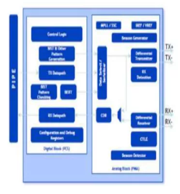
Block Diagram
Deliverables
- Datasheet
- Integration Guideline
- GDS or Phantom GDS
- Layer Map Table
- CDL Netlist for LVS
- LEF
- Verilog Behavior Model
- Liberty Timing Model
- DRC/LVS/ERC results
- RTL for Digital section
- Test Spec Document
Technical Specifications
Short description
V-by-One/LVDS Rx IP, Silicon Proven in SMIC 40LL
Vendor
Vendor Name
Maturity
In Production
Availability
Immediate
Related IPs
- Bluetooth Dual Mode v5.4 / IEEE 15.4 PHY/RF IP in GF 22nm (Silicon Proven)
- V-by-One/ LVDS Tx IP, Silicon Proven in SMIC 40LL
- JESD204B Tx-Rx PHY IP, Silicon Proven in SMIC 40LL
- eDisplay Port v1.4 Rx PHY IP in 40LL, Silicon Proven in SMIC 40LL
- ONFI 4.1 PHY IP (Silicon Proven in TSMC 12FFC)
- ONFi PHY 4.0 (FPHY+MDLL+SDLL Regulator) (Silicon Proven in TSMC 28HPC+)