MIPI CSI DSI C-PHY IP for TSMC (5nm, 6/7nm, 12/16nm, 22nm, 28nm, 40nm)

Overview

The MIPI C-PHY is designed and compliant with latest MIPI C-Phy Standards.

The MIPI C-PHY V1.2 improves throughput over a bandwidth-limited channel, allowing more data without an increased signaling clock. It is intended to be used for the camera interface (CSI-2 v1.3) and display interface (DSI-2 v1.0). The signaling interface uses a 3-phase transceiver that encodes 3-bit symbols over 3 wires. This is different from the two-wire differential “lane” used in D-PHY.

C-PHY was designed to coexist on the same IC pins as D-PHY so that dual-mode devices could be developed with low power signaling similar to DPHY. Arasan’s CPHY-DPHY combination provides a 3 channel C-PHY v1.2 and a four-lane D-PHY v1.2 in a single IP core. This allows a seamless implementation allowing the interface to D-PHY based sensors or C-PHY based sensors.

Symbol encoding effectively transfers 2.286 bits per symbol compared to 1.0 bits per lane for D-PHY. The C-PHY (v1.2) operates at 3GS/s, whereas the D-PHY V1.2 (2.5Gb/s).

A four-lane D-PHY V1.2 provides 10Gbps which enables:

  • 4K video at 30fps
  • 1080p at 120fps

A 3 channel C-PHY provides 17Gbps which enables:

  • 4K video at 60fps
  • 1080p at 240fps (for cool slow-motion videos)
Key Features

  • Support for MIPI® compliant C-PHY Specification Version 2.0 with backward compatibility for MIPI C-PHY v1.2 and v1.1
  • Supports up to 3 lanes/trios
  • Supports both high-speed and low-power modes
  • 80 Msps to 4.5 Gsps symbol rate per lane in C-PHY high-speed mode
  • Equivalent to 182.8 Mbps to 10.26 Gbps per lane in C-PHY high-speed mode
  • 10 Mbps data rate in low-power mode
  • Supports CSI-2, DSI, and DSI-2
  • Low power dissipation
  • Loopback testability (BIST) support
  • Supports standard PHY transceiver compliant to MIPI Specification
  • Supports standard PPI interface compliant to MIPI Specification
  • Supports asynchronous transfer at high speed mode with a symbols rate of 80-3000 MS/s on CPHY mode.
  • Supports synchronous transfer at high speed mode with a bit rate of 80-1500 Mb/s without deskew calibration and upto 2500 Mb/s with deskew calibration on DPHY mode.
  • Supports asynchronous transfer at low power mode with a bit rate of 10 Mb/s on both CPHY and DPHY
  • Spaced one hot encoding for Low power [LP] data
  • Supports maximum of three data lanes on CPHY mode and four data lanes and clock lane on DPHY mode .
  • Supports error detection mechanism for sequence errors and contentions.
  • Data lanes support transfer of data in high speed mode.
  • Supports ultra low power mode, high speed mode and control mode.
  • Has clock divider unit to generate clock for parallel data reception and transmission from and to the PPI.
  • Activates and disconnects high speed terminators for reception and transmission.
  • On-chip clock generation configurable for transmitter.
  • Testability for Analog Tx, Rx and PLL and DFE.
  • Process & Foundry:
  • Available in various foundry processes
  • No external (off-chip) components required
  • Can be ported to other processes

Benefits

  • Silicon proven
  • Extensive Quality Methodology

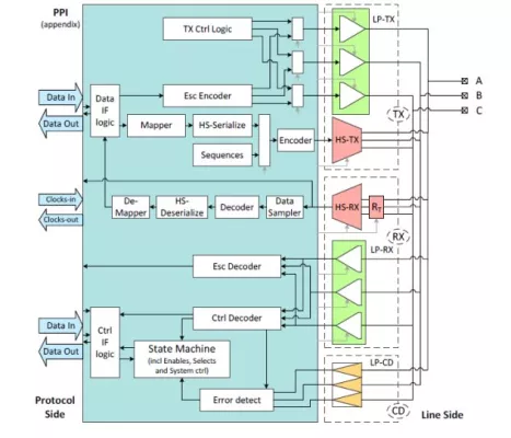
Block Diagram

MIPI CSI DSI C-PHY IP for TSMC (5nm, 6/7nm, 12/16nm, 22nm, 28nm, 40nm) Block Diagram

Video

Arasan CPHY-TestEvo Demo

Deliverables

  • GDS-II Database
  • LVS Netlist
  • Physical Abstract Models (LEF)
  • Timing Models (LIB)
  • Process Specific Integration Guide

Technical Specifications

Foundry, Node
TSMC 1 5nm, 6/7nm, 12/16nm, 22nm, 28nm, 40nm
Maturity
Silicon Proven
Availability
Now
TSMC
Pre-Silicon: 16nm
×
Semiconductor IP