Low power 9 bit cyclic ADC
Overview
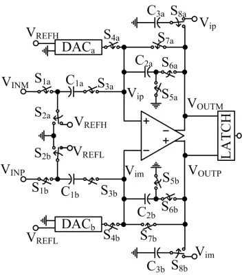
The ADC is a fully differential 9-bit cyclic ADC which utilizes 4-bit binary weighted array to obtain 9-bit resolution. Cyclic algorithm for the ADC conversion is used to reduce number of capacitors in the capacitor array and save layout area. The ADC is designed for suppression of the supply variation, even in the conversion cycle.
Key Features
- The ADC conversion is divided into three phases. In each of the phases three bits are obtained; in Phase I the three most significant bits are obtained (MSBs), in Phase II the three middle bits and in Phase III the three least significant bits (LSBs). The voltage swing at the output of the operational amplifier is adaptive and it depends on the conversion phase, accounting for the drop of supply voltage during the conversion cycle. Operational amplifier has a built-in slew rate (SR) detection circuit which dynamically controls the amplifier current and optimizes power consumption and speed.
Benefits
- Low power consumption, insensitivity to power supply variations
Block Diagram
Applications
- Low power applications, low sampling rate, ADC, energy harvesting systems
Deliverables
- Schematic and layout design(GDS) for chosen 180 nm technology
Technical Specifications
Short description
Low power 9 bit cyclic ADC
Vendor
Vendor Name
Foundry, Node
180 nm
Maturity
First Silicon
Availability
Q3/2016
UMC
Silicon Proven:
180nm
Related IPs
- 16 Bit 13 kS/s Cyclic ADC on XFAB XH018
- 12 Bit 17 kS/s Cyclic ADC on XFAB XH018
- 12 Bit 54 kS/s Cyclic ADC on XFAB XH018
- 11 Bit 100 kS/s Ultra-Low Power SAR ADC on GlobalFoundries 22FDSOI
- I2C Controller IP – Slave, SCL Clock, Parameterized FIFO, APB Bus. For low power requirements in I2C Slave Controller interface to CPU
- AHB Low Power Subsystem - ARM Cortex M0