Systolic FIR Filter Based FPGA
Abstract :
In this paper, we first review in detail the basic building blocks of reconfigurable devices, essentially, the field-programmable gate arrays, then we describes a high-speed, reconfigurable Systolic Finite Impulse Response Filter design implemented in the Virtex-II series of FPGAs. A description language of this filter is used for simulation and implemented using Xilinx's place and route tools. The simulation shows that the filter behaves as expected.
I. INTRODUCTION
As field programmable gate array (FPGA) technology has steadily improved, FPGAs have become alternatives to other technology implementations for high-speed classes of digital signal processing (DSP) applications.
In this paper, we first review in detail the basic building blocks of reconfigurable devices, essentially, the field-programmable gate arrays (FPGAs), then we describes a high-speed, reconfigurable, Systolic FIR filter design implemented in the Virtex-II series of FPGAs.
II. REPROGRAMMABLE COMPUTING AND THE FPGA ARCHITECTURE
Reconfigurable computing (RC) is computation using hardware that can adapt at the logic level to solve specific problems. Figure 1 shows the implementation spectrum in reconfigurable computing [1]. The spectrum is bounded by three axes symbolising performances, flexibility and cost. The figure clearly shows that ASIC gives high performance at cost of inflexibility, processor is very flexible but not tuned to the application and that RC hardware (FPGA) is a nice compromise.
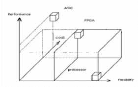
Fig 1. Implementation Spectrum
Reconfigurable hardware can be classified according to their granularity level, which are: the system level, the functional level and the logic level.
At system level the reconfiguration correspond to the programming of the computing resources such the different processors and memory space.
At functional level, the reconfiguration focuses on the interconnections between resources such as the different arithmetic modules.
Finally, at logic level the reconfiguration deals with the different L.U.Ts and the network of interconnects at bit level.
In reconfigurable computing we distinguish two types of reconfiguration as shown i n figure 2:
-
Static reconfiguration : the application is not running
-
Dynamic reconfiguration – application is modified in response to changing environmental issues.

Fig 2. Reconfiguration types
The basic structure of an FPGAs is array-based, meaning that each chip comprises a two dimensional array of logic blocks that can be interconnected via horizontal and vertical routing channels. An illustration of this type of architecture is shown in Figure 3.
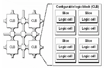
Fig 3. FPGA: Basic Structure
The features of a logic block (called a Configurable Logic Block (CLB) by Xilinx) shown in figure 4 is based on look-up tables (LUTs) . A LUT is a small one bit wide memory array, where the address lines for the memory are inputs of the logic block and the one bit output from the memory is the LUT output.
Modern VLSI FPGAs architecture shown in figure 5 are characterized by the integration of different building blocks [2] such as:
-
Logic cell (Combinational and Sequential) .
-
Dedicated Arithmetic Logic, processors,
-
Input/Ouput, JTAG, Gigabits transceiver blocks , etc...
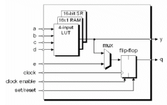
Fig 4. Configurable Logic Block (CLB)
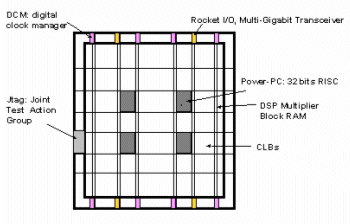
Fig 5. FPGA with embedded system functionality
III. SYSTOLIC FIR APPLICATIONS
Systolic system consists of an array of processing elements (typically multiplier-accumulator chips) in a pipeline structure that is used for applications such as image and signal processing. The "systolic array" introduced by H. T. Kung of Carnegie-Mellon in 1978, refers to the rhythmic transfer of data through the pipeline, like blood flowing through the vascular system [3].
Systolic approach can speed up a compute-bound computation in a relatively simple and inexpensive manner. A systolic array in particular achieves higher computation throughput without increasing memory bandwidth as shown in figure 6.
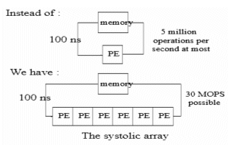
Fig 6. systolic array throughput
In [4], H.T.Kung proposed a family of systolic designs for the compute bound convolution problem, which is defined as follows:
- Given the sequence of weight
{w1 , w2 , . . . , wk}
- And the input sequence
{x1 , x2 , . . . , xk} ,
- Compute the result sequence
{y1 , y2 , . . . , yn+1-k}
- Defined by:
yi = w1 xi + w2 xi+1 + . . . + wk xi+k-1
From the proposed family of systolic designs, we have chosen the pure systolic convolution arrays without global data communication as illustrated in figure 7, in order to minimize global broadcasting and fan in problems inherent to FPGA designs.
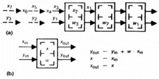
Figure 7: pure systolic convolution (a) and cell (b)
One such application is the well known finite impulse response (FIR) digital filter. The behavior of the finite impulse response filter can be described by the equation:
 (1)
(1)
where yt denotes the output at time t and xt represents the input at time t and ak are the filter coefficients.
The processing element of the 1D full systolic FIR is shown in fig 8. Both the x values and the accumulated results flow from left to right but at a different speed, while the coefficients stay in the cell.
An implementation of such filter is given in figure 9. The inner product processing element will take as inputs an accumulated sum from previous processing elements (yin), a filter coefficient (ai) and a sample value from the input stream (xin) and return two values: the xin is passed to xout and the yout is computed by performing the inner product calculation and adding it to the accumulated sum.
Registers are added at the inputs and outputs for pipelining in a way that makes sure the accumulated sums and x values stay in synchronisation.
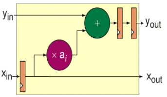
Fig 8. FIR processing element
An example of a four tap filter using this processing element is shown in fig 8. This is formed by simply replicating the processing element horizontally. The x input has to be delayed by one clock tick to synchronise with the y inputs. This filter has a much higher latency (8 ticks) than it direct implementation counterpart (semi systolic filter) known as a transversal FIR filter.
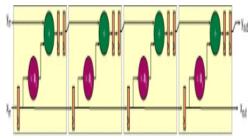
Fig 9. A 4 taps full systolic FIR filters
VHDL description of this filter is used for simulation and EDIF for implementation using Xilinx's place and route tools. The following code is a top level description of the filter which is made from an array of Multiply and Add modules (fs_tap) for scalability. By using dedicated Multiply Add DSP blocks (such as the DSP48), design efficiency is increased when correctly and optimally mapped to any FPGA-based DSP application.
-- Design Name: scale_fsyst_fir from A. GOUGAMlibrary ieee;
use ieee.numeric_bit.all;
use ieee.std_logic_1164.all;
entity scale_fsyst_fir is
generic (n : natural:=16;
n_tap : integer:= 10);--number of tapes set 10
port (dx_in ,dy_in, w_in : in std_logic_vector (n-1 downto 0);
ck : in std_logic;
qx_out, qy_out: out std_logic_vector (n-1 downto 0));
end scale_fsyst_fir;
architecture behavior of scale_fsyst_fir is
component fs_tap is
generic (n : natural);
port (fx_in, fy_in ,
fw_in : in std_logic_vector (n-1 downto 0);
ck : in std_logic;
fx_out, fy_out : out std_logic_vector (n-1 downto 0));
end component ;
type mat_a is array(1 to n_tap+1) of std_logic_vector (n-1 downto 0);
signal d,y, w: mat_a;
begin -- behavior
y(1) <= dy_in;--nil;
d(1) <= dx_in;
qx_out <= d(n_tap+1);
qy_out <= y(n_tap+1);
gen: for k in 1 to n_tap generate
w(1)<= x"0001"; -- coeff set to 1 for simplicity
w(2)<= x"0001"; w(3)<= x"0001";
w(4)<= x"0001"; w(5)<= x"0001";
t:fs_tap generic map (n) port map (d(k),y(k),w(k),ck,d(k+1),y(k+1));
end generate;
end behavior;
The VHDL simulation shows that the filter behaves as expected as shown on figure 10, a serie of unsigned number b[15:0] produced a same serie of filtered unsigned numbers q[15:0] . The first filtered data output is produced after the eigth clock pulse then, an output is produced every clock pulse. The coefficients Wi, of the filter have been set to 1 for simplicity.
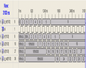
Fig 10. Simulation results using ISE 8i.
After configuration, ON CHIP debugging and verification is performed using ChipScope™ Pro tools which integrates logic analyzer hardware components with the target design inside Xilinx Virtex™. The ChipScope Pro tools communicate with these components and provides us with a complete logic analyzer. Figure 11 shows a block diagram of a ChipScope Pro system.
We can place the ICON, ILA, cores (collectively called the ChipScope Pro cores) into the design by generating the cores with the ChipScope Pro Core Generator and instantiating them into the VHDL source code.
The design is then placed and routed using the Xilinx ISE 8.1i implementation tools. Next, we download the bitstream into the device under test and analyzes the design with the ChipScope Pro Analyzer software.
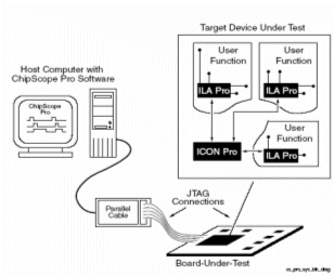
Fig 11. block diagram of a ChipScope Pro .
IV. CONCLUSION
Our study shows the suitability in using FPGAs for spatially parallel applications such as systolic filters. By illustrating a design methodology for digital filters[5], the advantages of using FPGAs for digital signal processing applications (DSP) are emphasized. Finally, further works on this subject is being carried out including :
- Making the filter parameters scalable as the number of taps.
- Extending this systolic FIR filter to real data acquisition.
- Comparing performances against existing optimized filter implementation from Xilinx's Core Generator in order to propose a real IP (Intellectual Property ) core for reuse .
V. REFERENCES
[1] R. David , “ Architecture reconfigurable dynamiquement pour applications mobiles”,Thèse,Université de Rennes, 2003.
[2] “The Design Worrior’s Guide to FPGAs Devices, Tools, and Flows”. ISBN 0750676043, Mentor Graphics Corp, 2004,
[3] H.T Kung, C.E Leiserson, “ Systolic Array for VLSI ”, Sparse Matrix Proc., 1979, pp. 256-282.
[4] H.T Kung, , “Why Systolic Architectures?”, Computer, Vol 15, N°1, jan 1982, pp. 37-46.
[5] A GOUGAM, A FARAH. “Systolic Arrays via dependancy graphs”. Journal of Technology (JOT), E.N.P El-Harrach, Algeria, 1994.
Related Semiconductor IP
- Multi Channel FIR Filter
- TX & RX FIR Filter specifically to support DSP Application
- Digital FIR filter with APB interface
- Serial FIR Filter
- Parallel FIR Filter
Related White Papers
- How to write an optimized FIR filter
- Learning from the Next-Gen Firewall
- FPGA comes back into its own as edge computing and AI catch fire
- Efficient FIR filtering with Bit Layer Multiply Accumulator
Latest White Papers
- Achieving Lower Power, Better Performance, And Optimized Wire Length In Advanced SoC Designs
- The pivotal role power management IP plays in chip design
- What tamper detection IP brings to SoC designs
- Analyzing Modern NVIDIA GPU cores
- RISC-V in 2025: Progress, Challenges,and What’s Next for Automotive & OpenHardware