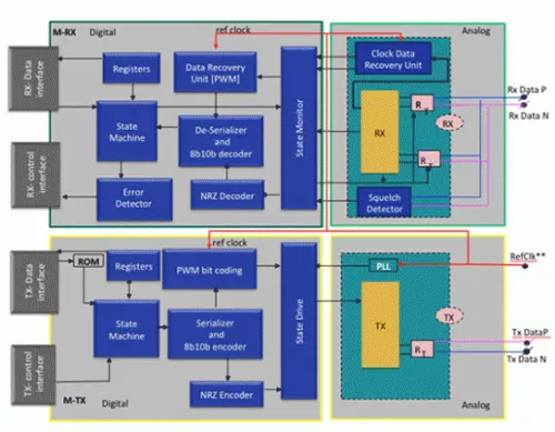
ACS-AIP-MPHY-28HK MIPI Specification Version 3.0 is a low pin count, power efficient, inter-chip serial interface with high bandwidth capabilities. A M-PHY configuration (LINK) consists of a minimum of two unidirectional lanes along with associated lane management logic. Each of the M-PHY lanes consists of a lane module (M-TX) that communicates to a corresponding module (M-RX) on the other chip via a serial interconnect that consists of two differential lines. The differential lines can carry both High-Speed (HS) and Low-Speed (LS) signals.
Arasan’s M-PHY’s are of Type 1, which apply to UFS, LLI and CSI-3 protocols. The M-PHY consists of analog transceivers, high speed PLL, data recovery units as well as the state-machine control — all in a single GDSII. The interface to the link protocol-specific controller (host or device) is compliant to the M-PHY RMMI specification, which allows seamless integration of the two IPs, namely the controller and the PHY, into the chip design.
Design Philisophy: Arasan’s approach to M-PHY design is end-to-end protocol specific. Different protocols have different requirements in terms of clocking. A single version of M-PHY that caters to all protocols can become prohibitively large and consume more power than necessary. Hence Arasan delivers the most area and power efficient implementation for each MIPI M-PHY protocol.
Arasan follows a rigorous practice of co-verifying the controllers and their corresponding PHY’s to ensure that they operate together as intended. These, together with Arasan’s software stacks, are mapped onto Arasan’s Hardware Validation Platforms, which are used for early compatibility and interoperability testing with the corresponding host/device platforms from Arasan and a number of MIPI contributor members. This minimizes end-to-end compatibility risk for customers.
MIPI M-PHY Designed For GF 28nm
Overview
Key Features
- •Compliant to MIPI Alliance Standard for M-PHY specification Version 3.0
- •Supports high speed data transfer G1A/B, G2A/B and G3A/B with data rates of up to 5830.4 Mbps
- •Supports M-PHY Type-I system
- •Support for reference clock frequencies of 19.2MHz/26MHz/38.4MHz/52MHz
- •Support for Clock and Data Recovery Options
- •Supports low speed transfer G0-G7 with a bit rate of up to 576 Mbps
- •PWM signalling for Low speed [LS] data
- •Supports error detection mechanism for sequence errors and contentions
- •Data lanes support transfer of data in high speed mode
- •Supports LS burst, HS burst, STALL, SLEEP, HIBERN8 states
- •Supports squelch detection
- •Has clock divider unit to generate clock for parallel data reception and transmission from and to the PIF (RMMI)
- •Activates and disconnects high speed terminators for reception and transmission
- •Supports standard PHY transceiver compliant to MIPI Specification •Supports standard PIF (RMMI) interface compliant to MIPI Specification.
- •On-chip clock generation configurable for either transmitter or a receiver
- •Testability for Tx, Rx and PLL
Benefits
- Compliant with MPHY and the relevant protocols standards
- Seamless interface to Arasan’s host and device controllers for those standards
- Configurable number of lanes
- Area and power efficient
Block Diagram

Deliverables
- User Guide and Integration Guides
- GDS-II
- CDL Netlist for LVS
- LVS reports
- DRC and Antenna reports
- LIB files
- LEF
- Scan-inserted Netlist for DFT
- Verification Environment with behavioral models.
Technical Specifications
Maturity
Silicon Proven
Availability
Now
Related IPs
- MIPI M-PHY Designed For TSMC 28nm
- MIPI M-PHY Designed For TSMC 28nm
- MIPI M-PHY G4 Designed For TSMC 28nm HPC+
- Self-contained cryptographic subsystem designed for PQC + classical, minimal integration effort, with SCA protection
- MIPI M-PHY
- HDMI 2.0 TX PHY 6Gbps in GF 28nm SLP 1.8V, East/West Poly Orientation