Low Power Successive-Approximation ADC 12.5 MS/s 12-Bit
Overview
This IP is a general purpose Analog to Digital Converter (ADC) for low-power applications. The converter is a charge-redistribution successive-approximation type converter, suitable for the entire Nyquist band.The key feature of this ADC is its low power consumption. This is achieved by using an energy efficient comparator and by making all circuitry dynamic. As a result, quiescent current in e.g. amplifiers is avoided, and the power consumption is fully proportional to the sample-rate. This property makes the ADC ideal for low duty-cycle sensor applications and other applications benefiting from low power consumption.The converter can operate in both single-ended and differential mode, making it suitable for a broad range of applications.
Key Features
- sample-rate up to 12.5 MS/s
- low power consumption,
- proportional to sample-rate:
- 1.2 mW @ 12.5 MS/s
- 12 uW @ 125 kS/s
- single-ended and differential mode
- 10.5 ENOB
- >78 dB SFDR (incl. THD)
- 0.17 mm2 in baseline 0.18 um CMOS
- rail-to-rail input range
- supports full Nyquist band
Benefits
- Scalable power, power consumption is linear with sample rate.
- When no clock signal the power consumption of the ADC is negligible.
- Well suited for porting to other technologies.
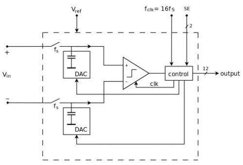
Block Diagram
Applications
- Low-power applications
- Sensor applications
- Radio baseband processing
Deliverables
- The IP deliverables package consist of
- GDS file
- Behavioral model
- Netlist
- Integration documentation.
Technical Specifications
Foundry, Node
CMOS180 XFAB
Maturity
Pre silicon
Availability
Summer 2012