USB 2.0 PHY Verification
Gary Miller, Freescale Semiconductor Inc
Austin, TX, USA
Abstract:
Although there are numerous USB Verification IPs (VIP) offered for the functional verification of the controller side of a high-speed-communication interface, there are few available for the Physical-layer (PHY) compliance testbench. Yet functional verification of the USB 2.0 PHY Physical Layer Macrocell can be an equally complex challenge due to the analog and digital content.
One of the challenges in a PHY verification is the fact that a PHY may have complex analog and digital circuits and a sophisticated logic interface to the PHY controller module. Another challenge is the fact that a PHY may have a myriad of implementation options that impact the operation and system topology. (Note that system topology refers to the role that the PHY plays in the network, such as master, slave, dual-role, and the related PHY functions that must be exercised as determined by the associated software stack.) These challenges may imply the need for a PHY level functional verification testbench.
In this paper we present a Vera-based reusable environment to verify a USB 2.0 PHY that addresses some of the problems of a typical PHY Verification. Thus, we present the developed VIPs such as monitors, response checkers and functional coverage object needed to be re-used for multiple PHY implementations, as well as potentially in an integrated Controller/PHY testbench.
Although the paper is based on a USB 2.0 System, the concepts developed could be used in other PHYs of interest such as Ethernet and PCI-Express.
1.0 Introduction:
The Universal Serial Bus (USB) is a serial bus standard to interface devices. First designed to allow connections to the PC without expansion cards, the USB became a de-facto communication standard for almost all electronic devices.
The USB communication is always initiated by a Host and responded by a Device. USB Hubs act as switches to expand the number of devices per Host. Special Onthe- Go (OTG) devices can act as either Host or Device and can change roles while connected to other OTG devices [6].
On its 2.0 Standard release, USB permits three speed of communicaiton Low Speed 1.5M bits/s, Full Speed 12 Mbits/s and High Speed 480 Mbits/s. At the high speed frequency it is difficult to synthesize HDL code without modification. That is why the USB Transceiver Macrocell Interface (UTMI) Standard is defined.
Comprising complex digital and analog design, the Macrocell or PHY may require as much verification as the controller unit of the USB interface. That’s why the Microcontroller Division (MCD) from Freescale decided to use advanced verification techiniques to verify the UTMI+ PHY as described in this paper.
The paper is divided as follows: Section 2.0 of this paper describes the Module Under Verification (MUV). Section 3.0 describe the Verification Plan for the PHY, it also describes methodology, testbench, verification flow and drivers used. Section 4.0 describes the planned stimulus and the randomization constraints used. Finally on section 5.0 we present the conclusions of this work and recommendation for future works.
2.0 Module Under Verification
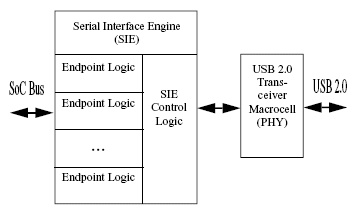
An implementation of USB 2.0 [1] comprises a Serial Interface Engine (SIE), sometimes referred to as a USB controller, and a Transceiver Macrocell. Figure 1 illustrates a peripheral USB controller and Transceiver Macrocell. A host or OTG controller will contain a list processing engine to handle the EHCI/OHCI/UHCI data structures [4] and [5].

Figure 1 Peripheral USB Controller and PHY
The USB 2.0 Transceiver Macrocell comprises the following:
-
Sophisticated logic to interface with an SIE for USB 2.0 host, device and OTG applications. The logic sub-blocks and SIE interface definition are defined in the reference documents [2] and [3].
-
High speed, full speed and low speed analog circuitry to interface with the USB cable. The design requirements are defined by reference document [1].
Throughout the document the term PHY will be used to refer to both the logic and analog portions of the USB 2.0 Transceiver Macrocell.
2.1 USB PHY Implementation Options
The USB PHY under verification has multiple implementation options based on if it is host, device or OTG controller, and if it is single or multi-ported1.
PHY implementations can support several data signaling rates such as high speed (HS), full speed (FS) and low speed (LS). In general, a host or OTG PHY supports all data signalling rates. In our case a device PHY will likely support one of these two options: HS/FS or LS only.
2.2 PHY Signal Interface
The interface between PHY and SIE for host, device and OTGimplementations is the UTMI+ interface with small internal changes to increase observability and controllability. Please refer to [3] for further information about the UTMI+ interface.
3.0 USB PHY Verification Plan
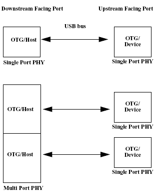
The USB PHY block is logically verified in a standalone testbench environment. In our case, the supported topology is shown in Figure 2.
The environment enables the verification of
-
Single or multi-port PHY implementations
-
Host, device or OTG PHY implementations
-
USB signal attributes of the device model using a mixed signal simulator.
-
Analog behavioral model correlation against the device model

Figure 2 Supported PHYs
3.1 Re-Use Strategy
The testbench is designed for re-use on the aforementioned objectives in every technology for which a PHY will be targeted. In the following sections a strategy to facilitate such broad re-use is described.
3.2 Upstream and Downstream PHY Testbench
The testbench comprises 2 PHYs connected via the USB bus as illustrated in Figure 2. The main purpose for this configuration is to be able to use behavioral or device models for the analog frontend of both PHYs. Having similar type analog frontend models communicate in Verilog (behavioral models) or analog models(device models) effectively masks USB signal representation differences between model types.
3.3 Custom USB Translator
PHY behavior models can use Verilog strenghs or other methods to represent the analog levels required by the USB bus, therefore a Custom USB Translator (CUT) is used to map USB signal representation to our designated internal standard. This translation allows the usage of a common, re-usable USB protocol monitor based on this standard, thus enabling response checkers to utilize transaction information published by the USB bus protocol monitor.
3.4 Strategy for Multi-Port PHY Implementations
The Multi-Port PHY is treated as two separate PHYs in the same environment. The testbench allows concurrent stimulus running on the two ports of the PHY. Therefore any stimulus can run on any port of the multi-port PHY.
3.5 Horizontal and Vertical Re-Use of PHY Verification IP
Testbench components designed for PHY verification, such as monitors, response checkers and functional coverage, needs to be re-used for multiple PHY implementations, as well as potentially in an integrated SIE/PHY testbench. Additionally, testbench components may need to be promoted to an SoC level testbench. The testbench and all Verification Components are created using a set of Vera Base Classes that together compounds the Freescale’s Verification library. System Verilog Assertions (SVAs) is used as well for freemonitoring and coverage.
3.6 Verification Methodology
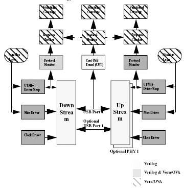
PHY verification is accomplished with a robust module level testbench. Figure 3 depicts the testbench.

Figure 3 Testbench
The following testbench components are used:
-
A clock driver for the SIE interface. The clock driver emulates the asynchronous nature of PHY operation.
-
Protocol monitors and/or drivers as appropriate for the SIE interface. The driver and protocol monitor requirements are extracted from reference documents [2] and [3].
-
A CUT to translate USB signal representation to our internal standard 32 state bus.
-
A protocol monitor for the USB bus. The protocol monitor requirements are extracted from reference document [1].
-
A response checker for the PHY for checking behavior predominantly at the transaction level on the UTMI+ and USB bus. The response checker requirements are extracted from reference documents [1], [2] and [3].
-
Directed and constrained random stimulus for the upstream and downstream PHYs. The stimulus requirements are extracted from reference documents [1], [2] and [3].
-
Functional coverage for tracking run-time coverage of intended coverage points.
3.7 Verification Flow
In general, the PHY verification flow can be described as follows:
-
Develop a generic understanding of the USB 2.0 and a detailed understanding of USB 2.0 PHY design and verification requirements.
-
Develop an understanding of the myriad of design implementation options and how they impact testbench and stimulus design.
-
Develop and document the verification guide to successfully accomplish PHY verification and re-use requirements. Annotation of specific sections of the reference documents are conducted to more thoroughly capture testbench and stimulus requirements.
-
Develop testbench components such as drivers, monitors, response checkers and functional coverage objects. Utilize brainstorming sessions prior to creation of verification IP.
-
Determine and develop functional coverage points at the frontend of the verification process.
-
Develop directed and constrained random stimulus. Use functional coverage reports to assess stimulus integrity and completeness.
-
Perform code coverage analysis to identify additional stimulus. Develop additional stimulus to improve code coverage as needed. The expectation is that 100% block and expression coverage including disposition are achieved.
-
Perform regressions on PHY database releases until bug rate decreases to acceptable level and there are no significant known bugs.
PHY verification is completed when these steps are successfully completed.
3.8 USB 2.0 Driver
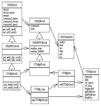
The USB 2.0 PHY driver is implemented for reuse in different levels of verification. Figure 4 shows the driver class diagram.
This driver provides an abstract interface, USB2DrvIf, and this interface allows the stimulus to get a command and run it without knowing specifics of the PHY being tested. Actually, as this is an abstract interface, it could be specialized for PHY, SIE or even SoC test.

Figure 4 USB 2.0 Driver Interface
4.0 Stimuli Development
The main objective of the stimulus is to create traffic through the PHY system to allow checking for the functional features. There can be Stimulus of two types:
-
Stimulus with access to both Upstream and Downstream ports, referred as global stimulus;
-
Stimulus with access just to one of the ports, referred as local stimulus;
Stimulus with access to both ports need to synchronize the transmission and reception of packets, but have freedom to perform as many transactions as necessary.
On the other hand, stimulus with access to just one of the ports will take advantage of the responder connected to the other PHY. The stimulus and responder obey some rules, e.g. the PHY acting as a host will always start a transaction and the PHY acting as a device will answer to such transaction. Thus, if connected to just one of the ports the stimulus needs to check for which port it is connected to, and act accordingly.
Thus, one of the following stimulus configuration are possible:
-
Upstream and Downstream PHYs connected to one global stimulus;
-
Upstream PHY and Downstream PHY each connected to a local Stimulus;
-
Upstream PHY connected to a local Stimulus and Downstream PHY connected to a Responder;
-
Upstream PHY connected to a Responder and Downstream PHY connected to a local Stimulus;
The transmission across the PHYs starts with the Stimulus/Responder acting as a Host, and the Stimulus/ Responder acting as a device responds to such transmission.
The Stimulus/Responder acting as a Host, in a normal transmission, should take the following steps:
-
creates a command to be executed;
-
sends the command to the USB2 Driver Interface which is responsible for transferring it to the PHY driver;
-
wait for the completion of such command;
-
check response for any expected result or send the subsequent command;
-
Repeat steps 1 to 4 until all commands are executed;
The Stimulus/Responder acting as a device, in a normal transmission, should take the following steps:
-
wait for transmission from downstream port;
-
decode received packet, and check for expected result or send the subsequent command;
-
create command to be send through the PHY;
-
send the command to the USB2 Driver Interface which is responsible for transmitting it to the PHY driver;
-
repeat steps 1 to 4 until all commands are executed or end of simulation is indicated at the received packet;
Note that since the USB2 Driver interface is abstract, it independent of the PHY, and therefore can be used in any testbench configuration, such as SoC or SIE + PHY.
4.1 Randomization
PHY verification simulations comprises random simulations as well as directed test simulations. The random stimulus achieves coverage of the targeted functional coverage attributes. The directed stimulus covers basic cases for debug, connectivity checking and corner cases not easily targeted by random stimulus. Directed stimulus also contains some amount of randomization, such as test order and packet data.
The stimulus is not intended to represent realistic USB packet IDs (PIDs) and fields, as this is not necessary for PHY verification. One exception is that the SOF PID is critical to PHY verification and thus will be required.
The following parameters are randomized:
-
Reference clock skew between each PHY: +/-12 bits for 1024 byte packets.
-
Skew between dm and dp for PHY transmissions - max skew of 100 ps.
-
Reference clock jitter during receive.
-
Connection/disconnection of upstream facing PHY.
-
Reset of downstream facing PHY.
-
Inter-packet delay.
-
Packet signaling rate - At the occurrence of each USB reset the signalling rate should be randomly changed.
-
Randomize packets size from 0 (or 1) to above 1024 bytes on parallel and serial interface, while assuring that overruns do not occur inadvertently.
-
Packet field data on parallel and serial interface.
-
Bus size of 8 or 16 for packet transmit/receive.
-
Clock skew between each PHY beyond +/-12 bits for 1024 byte packets.
-
EOP not on a byte boundary.
-
Bit stuffing errors;
-
Generate SOF PID.
-
Ocurrence of Suspend state.
-
Occurrence of resume state
-
Change direction between the upstream and downstream PHYs after a random number of packets.
-
Generate error with excessive reference clock skew and/or jitter.
-
Generation of LS keep-alive packet.
-
Generation of HS keep-alive packet.
-
Generate a dribble bit i.e. last bit before an EOP that can become stretched and produce a sixth bit that does not require bit stuffing.
-
Randomly generate SYNC field length for HS.
5.0 Conclusions and Recommendations
The state of the art PHYs requires that we build a dedicated testbench to check for the PHY behavior. There are not a good offerings of VIPs for this purpose.
We could find several USB drivers and even UTMI drivers but always focusing on the SIE verification.
The modular nature of the testbench and the usage of HLVL helped on the easy and fast setup of the environment as well as on the reuse of the environment for further projects. Therefore one of our conclusions is that the usage of a well structured Object Oriented Base Classes is very important for reuse.
The usage of abstract interface is very powerful while it allows the stimulus to be used in other environments in the case on the SIE+PHY environment or at the SoC level.
The connection of two PHYs is very interesting while it abstracts the details of the USB bus and allows the usage of the testbench for analog level simulation. This technique should be used with care since it can mask symbiotics problems hidden in the two modules.
Although we still didn’t start the mixed signal work, this task is extremely important in these kind of modules, and should be a complement to the task that we have just presented.
6.0 References
[1] Universal Serial Bus Specification Revision 2.0 (USB specification)
[3] UTMI+ Specification Revision 1.0 (UTMI+)
[6] OTG Supplement
Related Semiconductor IP
- USB 2.0 Verification IP
- USB 2.0 Verification IP
- USB 2.0 Hi-Speed OTG Controller version 4 with Active Clock Gating to save active power
- USB 2.0 Hi-Speed OTG Controller Subsystem w/AHB Interface Supporting HSIC (config. as Device only or Full Speed only)
- USB 2.0 Device Controller version 4 with Active Clock Gating to save active power
Related White Papers
- Mixed-Signal Verification for USB 2.0 Physical Layer IP
- Low Power USB 2.0 PHY IP for High-Volume Consumer Applications
- Which USB is Right for Your Application? (Part 2)
- USB 3.1 Gen 2 Brings Higher Data Rates with Architecture Improvements
Latest White Papers
- Achieving Lower Power, Better Performance, And Optimized Wire Length In Advanced SoC Designs
- The pivotal role power management IP plays in chip design
- What tamper detection IP brings to SoC designs
- Analyzing Modern NVIDIA GPU cores
- RISC-V in 2025: Progress, Challenges,and What’s Next for Automotive & OpenHardware