PCI IP
Welcome to the ultimate PCI IP hub! Explore our vast directory of PCI IP
All offers in
PCI IP
Filter
Compare
559
PCI IP
from 53 vendors
(1
-
10)
-
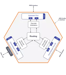
PCIe 6.2 Switch
- 1 upstream port, up to 7 downstream ports
- Up to 128 lanes
- PCIe TLP routing: Configuration, Memory Write/Read, I/O and Messages Packets
- L1 and wake-up events forwarding
-
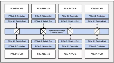
PCIe 7.0 Switch
- Configurable from PCIe 7.0 x8/ PCIe6x16 @1GHz clock down to PCIe 5.0 x1
- Highly scalable with up to 31 configurable external or embedded endpoints
- Configurable Egress Buffer for non-blocking output queueing switch performance
- Flit mode to non-Flit mode conversion
- Low power optimized
- Superior performance through a nonblocking architecture
- Minimized footprint
-
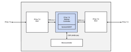
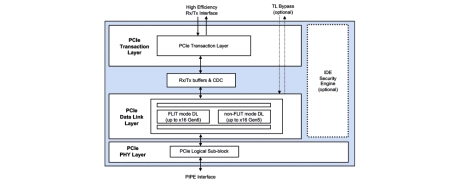
PCIe 7.0 Retimer Controller with CXL Support
- Supports PCIe 7.0 128 GT/s speeds at up to x16 lanes
- CXL 3.0 aware
- Supports PIPE 6.2.1 compatible PHYs
- Optimized for low latency
- Highly-configurable equalization algorithms and adaptive behaviors
-
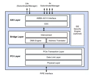
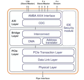
PCIe 7.0 Controller with AXI
- Optimized for high-bandwidth efficiency at data rates up to 128 GT/s
- Separate native TX/RX data path separating posted/Non posted/completion traffic
- Handles up to 4 TLPs per cycle
- Advanced PIPE modes and port bifurcation
-
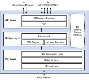
PCIe 7.0 Controller
- Optimized for high-bandwidth efficiency at data rates up to 128 GT/s
- Separate native TX/RX data path separating posted/Non posted/completion traffic
- Handles up to 4 TLPs per cycle
- Advanced PIPE modes and port bifurcation
-
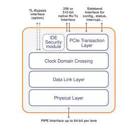
PCIe 6.1 Controller
- Designed to the latest PCI Express 6.1 (64 GT/s), 5.0 (32 GT/s), 4.0 (16 GT/s), 3.1/3.0 (8 GT/s), and PIPE 6.x (8, 16, 32, 64 and 128-bit) specifications
- Supports SerDes Architecture PIPE 10b/20b/40b/80b width
- Supports original PIPE 8b/16b/32b/64b/128b width
- Compliant with PCI-SIG Single-Root I/O Virtualization (SR-IOV) Specification
- Supports multiple virtual channels (VCs) in FLIT and non-FLIT modes
- Supports Endpoint, Root-Port, Dual-mode, Switch port configurations
-
PCIe 5.0 Controller with AXI
- Comprises complete PCIe 5.0 interface subsystem with Rambus PCIe 5.0 PHY
- Supports the PCI Express 5.0 rev. 1.0 (32 GT/s), 4.0 (16 GT/s), 3.1/3.0 (8 GT/s) and PIPE (8, 16, 32 and 64-bit) specifications
- Supports the PCI-SIG Single-Root I/O Virtualization (SR-IOV) Specification
- Supports Endpoint, Root-Port, Dual-mode configurations
-
PCIe 5.0 Controller
- Comprises complete PCIe 5.0 interface subsystem with Rambus PCIe 5.0 PHY
- Supports the PCI Express 5.0 rev. 1.0 (32 GT/s), 4.0 (16 GT/s), 3.1/3.0 (8 GT/s), and PIPE 5.x (8, 16, 32 and 64-bit) specifications
- Compliant with PCI-SIG Single-Root I/O Virtualization (SR-IOV) Specification
- Supports Endpoint, Root-Port, Dual-mode, Switch port configurations
-
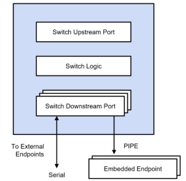
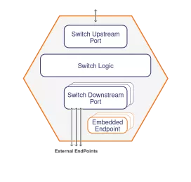
PCIe 5.0 Multi-port Switch
- Fully transparent design eliminates the need for Host configuration and management software
- Built-in support for PIPE-attached embedded endpoints (including 64-bit PIPE) for reduced BoM, latency, and power
- Seamless implementation on ASIC and FPGA with same RTL code base, up to x8 Gen4 per port on FPGA (or x16 Gen3)
- Lowest latency switching logic on the market (2 clock cycles)
-
PCIe Switch for USB4
- Fully transparent design eliminates the need for Host configuration and management software
- Built-in support for PIPE-attached embedded endpoints (including 64-bit PIPE) for reduced BoM, latency, and power
- Seamless implementation on ASIC and FPGA with same RTL code base, up to x8 Gen4 per port on FPGA (or x16 Gen3)
- Lowest latency switching logic on the market (2 clock cycles)