Memory Interface IP
Memory Interface IP cores support a wide range of memory types and standards, including DDR IP (Double Data Rate), GDDR IP (Graphics Double Data Rate), HBM IP (High Bandwidth Memory), and LPDDR IP (Low Power DDR), ensuring optimal performance in applications such as gaming, data centers, and mobile devices. NVM Express IP offers high-speed, low-latency storage interface for solid-state drives, while ONFI IP supports NAND flash memory communication. Additionally, SAS IP (Serial Attached SCSI) and SATA IP (Serial ATA) enable reliable, high-performance storage solutions, and SD/eMMC IP cores facilitate efficient data transfer for embedded systems.
All offers in
Memory Interface IP
Filter
Compare
1,380
Memory Interface IP
from 80 vendors
(1
-
10)
-
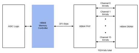
HBM4 Memory Controller
- Supports HBM4 memory devices
- Supports all standard HBM4 channel densities (up to 32 Gb)
- Supports up to 10 Gbps/pin
- Refresh Management (RFM) support
- Maximize memory bandwidth and minimizes latency via Look Ahead command processing
- Integrated Reorder functionality
-
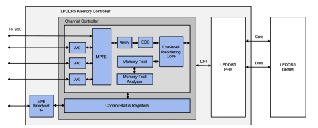
LPDDR5T / LPDDR5X / LPDDR5 Controller
- Support for all LPDDR5T/5X/5 devices
- Bank management logic monitors status of each bank
- Queue-based user interface with reordering scheduler
- Look-ahead activate, precharge, and auto-precharge logic
- Parity protection for all stored control registers
- PHY interface based on DFI 5.1 standard
-
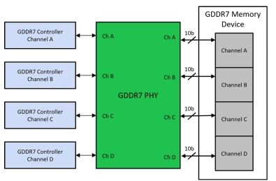
GDDR7 Memory Controller
- Supports up to 40 Gbps per pin operation
- 2.5 GHz CK4 clock
- 1.25 GHz controller clock
- Internal data path 32x memory width (i.e. 256 bits for 8-bit memory)
- Optimized for high efficiency and low latency across a wide range of traffic scenarios (random/sequential, short/long bursts, etc.)
- Optimized command sequence for highest bus utilization including per-bank refresh scheduling: single queue structure handles look-ahead activates/ precharges and read/write ordering for minimal latency
-
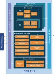
TSMC CLN4P 4nm DDR5 PHY - 6400Mbps
- Supports DDR5
- DFI 5.1 compliant
- Supports x4, x8 and x16 DRAMs
- Up to 72 bits wide and up to 4 ranks
-
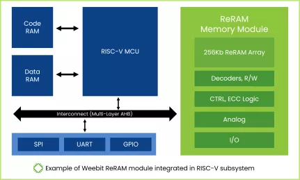
ReRAM NVM in SkyWater 130nm CMOS
- Technology: 130nm, SkyWater S130
- Mask Adder: 2
- Supply Voltage: 1.8V Read, 1.8V+3.3/3.6V Program
- Read Access Time: <20nsec
- Operation Temp.: -40°C - 125°C (can be extended to -55°C)
- Capacity: 256 Kbit (can be customized for 128Kbit - 2Mbit)
- Data Bus Width (Read): 32-bit (can be customized to 16-bit to 128-bit)
-
LPDDR5X DDR Memory Controller
- JEDEC LPDDR5X/LPDDR5 devices compatible
- Data rates up to 8533Mbps
- Multiple ARM AMBA AXI4/AHB/APB & Custom interfaces
-
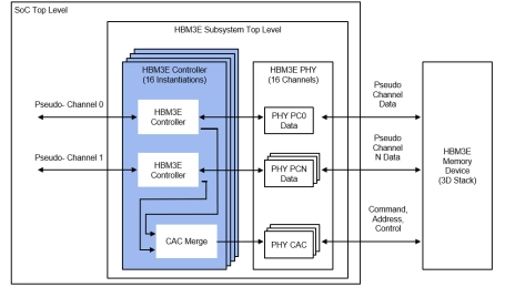
HBM3E/3 Memory Controller
- Supports HBM3E / HBM3 memory devices
- Supports all standard HBM3 channel densities (up to 32 Gb)
- Supports up to 9.6 Gbps/pin (HBM3E) or 8.4 Gbps/pin (HBM3)
- Refresh Management (RFM) support
- Maximizes memory bandwidth and minimizes latency via Look-Ahead command processing
- Integrated Reorder functionality
-
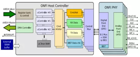
ONFI 5.0 PHY
- The PHY design supports the newly introduced NV-LPDDR4 mode along with SDR, NV_DDR, and NV_DDR2, NV_DDR3 mode.
-
ONFI 5.0 NAND FLASH Controller Compliant to JEDEC
- ONFI v5.0 compliant + Up to 2.4GByte/s.
- All I/O modes implemented + SDR + NV-DDR + NV-DDR2/3 + NV-LPDDR4
- Wide hardware support + Four 8-bit data paths + 8 NAND targets each + Data bus inversion.
- Full PLL support + PLL within PHY + 10MHz SDR + 1.2GHz NV-LPDDR4 + Everything in between

-
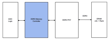
DDR3 Controller
- Maximizes bus efficiency via look-ahead command processing, bank management, auto-precharge and additive latency support
- Latency minimized via parameterized pipelining
- Achieves high clock rates with minimal routing constraints
- Supports full-rate and half-rate clock operation
- Multi-mode controller support