GDDR IP
Welcome to the ultimate HBM IP hub! Explore our vast directory of HBM IP
All offers in
GDDR IP
Filter
Compare
39
GDDR IP
from 7 vendors
(1
-
10)
-
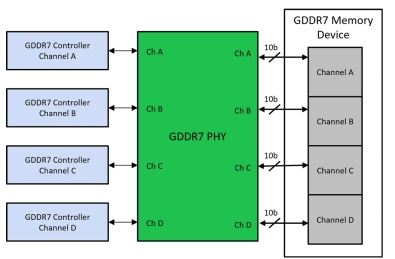
GDDR7 Memory Controller
- Supports up to 40 Gbps per pin operation
- 2.5 GHz CK4 clock
- 1.25 GHz controller clock
- Internal data path 32x memory width (i.e. 256 bits for 8-bit memory)
- Optimized for high efficiency and low latency across a wide range of traffic scenarios (random/sequential, short/long bursts, etc.)
- Optimized command sequence for highest bus utilization including per-bank refresh scheduling: single queue structure handles look-ahead activates/ precharges and read/write ordering for minimal latency
-
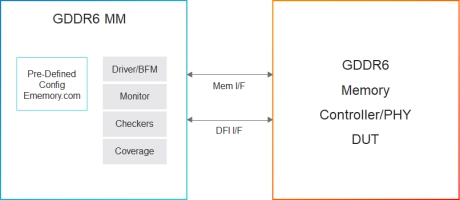
GDDR6 Memory Controller IP
- JEDEC GDDR6 standard JESD250B
- Fast frequency switching
- Flexible Configuration
-
GDDR6 PHY
- Single configuration supports one GDDR6 device per channel (coplanar) or two GDDR6 devices per channel (clamshell)
- DFI PHY Independent Mode for initialization and training
- Adaptive and continuous timing recovery
- Internal and external datapath loop-back modes
- Transmit crosstalk cancelation of immediate neighbors
- Per-bit DFE, CTLE, and FFE equalization
-
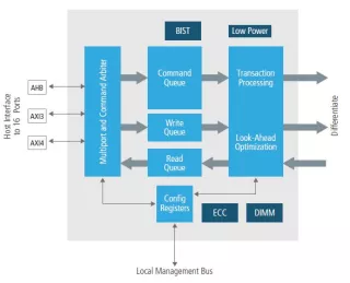
GDDR6 Controller
- In-line SEC/DED ECC
- Supports advanced RAS features including error scrubbing, parity, etc.
- Compatible with GDDR6 devices compliant to JESD250b
- Single and multi-port host options for Arm® AMBA®4, AMBA 3 AXI, and low-latency Denali interfaces
- QoS features allow command prioritization
- Flexible paging policy
-
GDDR5 Controller - Verifies memory compliance, boosts performance, and ensures reliability
- The GDDR5 Memory Controller Verification IP (VIP) is a robust solution designed to verify the compliance and performance of GDDR5 memory controllers. It ensures adherence to GDDR5 specifications, enabling high-speed data transfers, low latency, and power efficiency for advanced systems.
- This VIP is vital for applications requiring high data throughput and low latency, such as GPUs, gaming consoles, VR systems, HPC, AI accelerators, and data centers. It ensures reliable, high-performance memory operations across a variety of demanding use cases

-
GDDR4 Controller - Validates high-speed memory controllers for efficiency and reliability
- The GDDR4 Controller Verification IP (VIP) ensures robust simulation and validation of GDDR4 memory controllers in SoC designs. Supporting high-speed data transfers, protocol compliance, and power management, it simplifies testing and optimizes system performance.
- Ideal for high-performance applications, GDDR4 VIP enhances GPU, HPC, gaming consoles, and embedded systems. Its broad use spans automotive, AI, video processing, networking, and consumer electronics, ensuring efficient memory operations across industries
-
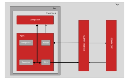
Simulation VIP for GDDR6
- Speed
- Supports up to 16Gbps with current vendor datasheets
- Device Density
- Supports a wide range of device densities from 8Gb to 32Gb
-
GDDR7 Synthesizable Transactor
- Supports GDDR7 memory devices from all leading vendors.
- Supports 100% of GDDR7 protocol draft JEDEC specification.
- Supports all the GDDR7 commands as per the specs.
- Supports 4 separate independent channels with point-to-point interface for data, address and command.

-
GDDR6 Synthesizable Transactor
- Supports 100% of GDDR6 protocol standard JESD250, JESD250A, JESD250B and JESD250C specification with version 3.12
- Supports all the GDDR6 commands as per the specs
- Supports 2 separate independent channels with point-to-point interface for data, address and command
- Supports double data rate (DDR) or quad data rate (QDR) data
-
GDDR5 Synthesizable Transactor
- Supports 100% of GDDR5 protocol standard JESD212C
- Supports all the GDDR5 commands as per the specs
- Supports all types of timing and protocol violation detection
- Supports up to 8GB device density
