LPDDR IP
All offers in
LPDDR IP
Filter
Compare
181
LPDDR IP
from 23 vendors
(1
-
10)
-
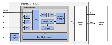
LPDDR5T / LPDDR5X / LPDDR5 Controller
- Support for all LPDDR5T/5X/5 devices
- Bank management logic monitors status of each bank
- Queue-based user interface with reordering scheduler
- Look-ahead activate, precharge, and auto-precharge logic
- Parity protection for all stored control registers
- PHY interface based on DFI 5.1 standard
-
LPDDR5X DDR Memory Controller
- JEDEC LPDDR5X/LPDDR5 devices compatible
- Data rates up to 8533Mbps
- Multiple ARM AMBA AXI4/AHB/APB & Custom interfaces
-
LPDDR4X / LPDDR4 Controller
- Maximizes bus efficiency via look-ahead command processing, bank management, and auto-precharge
- Latency minimized via parameterized pipelining
- Achieves high clock rates with minimal routing constraints
- Supports full-rate, half-rate and quarter-rate clock operation
- Multi-mode controller support
-
DDR4/3, LPDDR5x/5/4x/4 Memory Controller IP
- Compliant with JEDEC standard for LPDDR5/4/3, DDR4/3
- DRAM rank of up to 4
- Lock-step-based controlling of multiple DRAM devices up to x64 DQ width
- Support for dynamic DRAM frequency scaling

-
LPDDR5/4x/4 combo PHY on 14nm, 12nm
- JESD209-5A(LPDDR5), JESD209-4C(LPDDR4), JESD209-4-1(LPDDR4X) compliant
- Operating speed up to 6400Mbps in LPDDR5, 4266Mbps in LPDDR4X
- Multiple DFICLK : CK :WCK ratios

-
LPDDR5X/5/4X/4 Memory Controller IP
- Intensive DRAM Utilization
- Ultra Low Power Consumption
- Extremely Low Latency
- Safety & Security
-
LPDDR5X/5/4X/4 combo PHY at 12nm
- Compliant with JEDEC JESD209-5C for LPDDR5x/5/4x/4 with PHY standards
- Delivering up to 8533Mbps
- DFI 5.1 specification PHY Interface Compliant
- Support up to 4 ranks

-
LPDDR5X/5/4X/4 PHY for 16nm
- Compliant with JEDEC standards for LPDDR5/4x/4 with PHY standards
- DFI 5.0 Interface Compliant
- Supports up to 4 ranks
-
LPDDR5/4x/4 PHY IP for Samsung 14LPU
- Compliant with PHY standards
- Flexible Configuration
- Maximum data rates
-
LPDDR4x/4 PHY IP for 22nm
- Compliant for JEDEC standards for LPDDR4x/4 with PHY standards
- DFI Interface Compliant
- Supports 1,2, or 4 ranks
- Multiple frequency states
