LPDDR5 IP
Welcome to the ultimate LPDDR5 IP hub! Explore our vast directory of LPDDR5 IP
All offers in
LPDDR5 IP
Filter
Compare
105
LPDDR5 IP
from 15 vendors
(1
-
10)
-
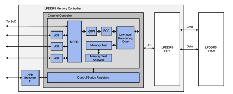
LPDDR5T / LPDDR5X / LPDDR5 Controller
- Support for all LPDDR5T/5X/5 devices
- Bank management logic monitors status of each bank
- Queue-based user interface with reordering scheduler
- Look-ahead activate, precharge, and auto-precharge logic
- Parity protection for all stored control registers
- PHY interface based on DFI 5.1 standard
-
LPDDR5X DDR Memory Controller
- JEDEC LPDDR5X/LPDDR5 devices compatible
- Data rates up to 8533Mbps
- Multiple ARM AMBA AXI4/AHB/APB & Custom interfaces
-
DDR4/3, LPDDR5x/5/4x/4 Memory Controller IP
- Compliant with JEDEC standard for LPDDR5/4/3, DDR4/3
- DRAM rank of up to 4
- Lock-step-based controlling of multiple DRAM devices up to x64 DQ width
- Support for dynamic DRAM frequency scaling

-
LPDDR5/4x/4 combo PHY on 14nm, 12nm
- JESD209-5A(LPDDR5), JESD209-4C(LPDDR4), JESD209-4-1(LPDDR4X) compliant
- Operating speed up to 6400Mbps in LPDDR5, 4266Mbps in LPDDR4X
- Multiple DFICLK : CK :WCK ratios

-
LPDDR5X/5/4X/4 Memory Controller IP
- Intensive DRAM Utilization
- Ultra Low Power Consumption
- Extremely Low Latency
- Safety & Security
-
LPDDR5X/5/4X/4 combo PHY at 12nm
- Compliant with JEDEC JESD209-5C for LPDDR5x/5/4x/4 with PHY standards
- Delivering up to 8533Mbps
- DFI 5.1 specification PHY Interface Compliant
- Support up to 4 ranks

-
LPDDR5X/5/4X/4 PHY for 16nm
- Compliant with JEDEC standards for LPDDR5/4x/4 with PHY standards
- DFI 5.0 Interface Compliant
- Supports up to 4 ranks
-
LPDDR5/4x/4 PHY IP for Samsung 14LPU
- Compliant with PHY standards
- Flexible Configuration
- Maximum data rates
-
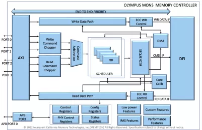
DDR/LPDDR Controller
- Sideband and in-line SEC/DED ECC
- Supports advanced RAS features including error scrubbing, parity, etc.
- Compliant to LPDDR5/4X/4/3 and DDR5/4/3 protocol memories
- Memory controller interface complies with DFI standards up to version 5.0
- Priority per command on Arm® AMBA® 4 AXI, AMBA 3 AXI
-
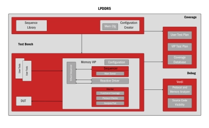
LPDDR5 Controller - Validates memory controllers for high-speed, power-efficient performance
- LPDDR5 Verification IP (VIP) is a tool designed to simulate and validate the functionality of LPDDR5 memory controllers. It ensures compliance with LPDDR5 specifications, covering high-speed data transfer, power management, error detection, and system integration.
- LPDDR5 VIP is essential across various industries, enabling high-performance systems to function optimally. It is utilized in mobile devices, automotive systems, high-performance computing, AI/ML, and more, ensuring efficient memory interfaces in diverse applications