DDR IP
DDR IP (Double Data Rate Interface) cores support high-speed data transfer for various types of DDR memory, including DDR3, DDR4, and DDR5, ensuring optimal performance for applications in computing, mobile devices, automotive systems, and embedded solutions. DDR IP cores offer features such as low latency, high bandwidth, and power efficiency.
All offers in
DDR IP
Filter
Compare
657
DDR IP
from 34 vendors
(1
-
10)
-
TSMC CLN4P 4nm DDR5 PHY - 6400Mbps
- Supports DDR5
- DFI 5.1 compliant
- Supports x4, x8 and x16 DRAMs
- Up to 72 bits wide and up to 4 ranks
-
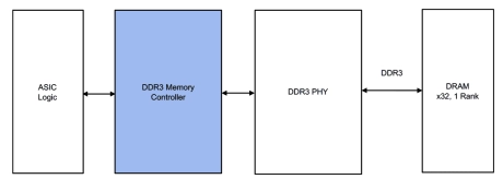
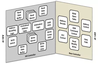
DDR3 Controller
- Maximizes bus efficiency via look-ahead command processing, bank management, auto-precharge and additive latency support
- Latency minimized via parameterized pipelining
- Achieves high clock rates with minimal routing constraints
- Supports full-rate and half-rate clock operation
- Multi-mode controller support
-
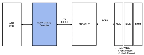
DDR4 Controller
- Maximizes bus efficiency via look-ahead command processing, bank management, auto-precharge and additive latency support
- Latency minimized via parameterized pipelining
- Achieves high clock rates with minimal routing constraints
- Supports half-rate and quarter-rate clock operation
- Supports DDR4 SDRAM 3DS device configurations
-
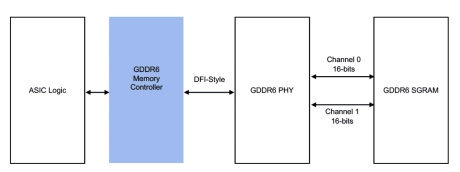
GDDR6 Controller
- Supports up to 24 Gb/s per pin operation
- Can handle two x16 GDDR6 channels with one controller or independently with two controllers
- Supports x8 or x16 clamshell mode
- Queue-based interface optimizes performance and throughput
- Maximizes memory bandwidth and minimizes latency via Look-Ahead command processing
- Automatic retry on transactions where EDC error detected
-
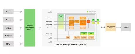
DDR4/3, LPDDR5x/5/4x/4 Memory Controller IP
- Compliant with JEDEC standard for LPDDR5/4/3, DDR4/3
- DRAM rank of up to 4
- Lock-step-based controlling of multiple DRAM devices up to x64 DQ width
- Support for dynamic DRAM frequency scaling
-
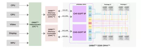
LPDDR5X/5/4X/4 combo PHY at Samsung SF5A
- Compliant for JEDEC standards for LPDDR5X/5/4X/4 with PHY standards
- DFI 5.1 specification PHY Interface Compliant
- Support up to 4 ranks
- x16 and x32 channel support

-
High Performance DDR5/4/3 Memory Controller
- Compliant with AXI4 Specification
- Compliant with DFI 3.1 Specification
- Compliant with JEDEC DDR3, DDR3L, DDR4 and DDR5 standards
- Supports 64, 32, 16 and 8 bit Memory SDRAM for DDR3L, DDR4 and DDR5
-
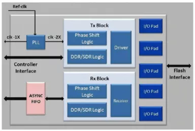
ONFI 3.2 NV-DDR2 PHY in GDSII
- Compliant to ONFI revision 3.2 standard
- Supports NV-DDR2 mode of operation supporting up to 266MHz or 566MT/s
- Supports NV-DDR mode of operation supporting up to 100MHz
- Supports legacy Asynchronous devices operating from 10MHz to 50MHz
-
LPDDR5X/5/4X/4 combo PHY at 7nm
- Unbeatable performance-driven and low-power-driven PPA
- Ultra-low read/write latency with programmable PHY boundary timing
- Channel equalization with FFE and DFE
-
GDDR6 Memory Controller IP
- JEDEC GDDR6 standard JESD250B
- Fast frequency switching
- Flexible Configuration
