DDR5 IP
Welcome to the ultimate DDR5 IP hub! Explore our vast directory of DDR5 IP
All offers in
DDR5 IP
Filter
Compare
514
DDR5 IP
from 23 vendors
(1
-
10)
-
TSMC CLN4P 4nm DDR5 PHY - 6400Mbps
- Supports DDR5
- DFI 5.1 compliant
- Supports x4, x8 and x16 DRAMs
- Up to 72 bits wide and up to 4 ranks
-
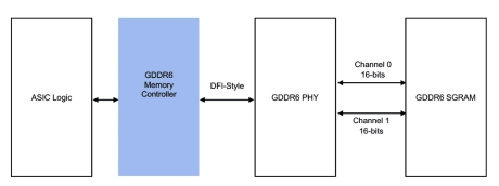
GDDR6 Controller
- Supports up to 24 Gb/s per pin operation
- Can handle two x16 GDDR6 channels with one controller or independently with two controllers
- Supports x8 or x16 clamshell mode
- Queue-based interface optimizes performance and throughput
- Maximizes memory bandwidth and minimizes latency via Look-Ahead command processing
- Automatic retry on transactions where EDC error detected
-
LPDDR5X/5/4X/4 combo PHY at Samsung SF5A
- Compliant for JEDEC standards for LPDDR5X/5/4X/4 with PHY standards
- DFI 5.1 specification PHY Interface Compliant
- Support up to 4 ranks
- x16 and x32 channel support

-
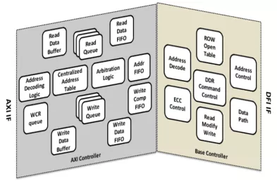
High Performance DDR5/4/3 Memory Controller
- Compliant with AXI4 Specification
- Compliant with DFI 3.1 Specification
- Compliant with JEDEC DDR3, DDR3L, DDR4 and DDR5 standards
- Supports 64, 32, 16 and 8 bit Memory SDRAM for DDR3L, DDR4 and DDR5
-
LPDDR5X/5/4X/4 combo PHY at 7nm
- Unbeatable performance-driven and low-power-driven PPA
- Ultra-low read/write latency with programmable PHY boundary timing
- Channel equalization with FFE and DFE
-
GDDR6 Memory Controller IP
- JEDEC GDDR6 standard JESD250B
- Fast frequency switching
- Flexible Configuration
-
LPDDR5X/5/4X/4 PHY IP for 12nm
- Compliant with JEDEC standards for LPDDR5X/5/4X/4 with PHY standards
- DFI 5.0 Interface Compliant
- Supports up to 4 ranks
- Multiple frequency states

-
GDDR6 PHY IP for 12nm
- JEDEC JESD250 compliant GDDR6 support
- X16 mode, X8 mode, and pseudo-channel mode
- Low frequency RDQS mode support
-
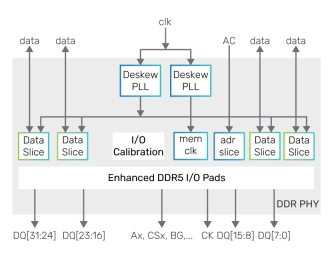
DDR PHY
- DDR5/4/3 training with write-leveling and data-eye training
- Optional clock gating available for low-power control
- Internal and external datapath loop-back modes
- I/O pads with impedance calibration logic and data retention capability
- Programmable per-bit (PVT compensated) deskew on read and write datapaths
- RX and TX equalization for heavily loaded systems
-
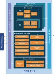
DDR5/4 PHY for TSMC 7nm
- Application optimized configurations for fast time to delivery and lower risk
- Memory controller interface complies with DFI standards up to 5.0
- Internal and external datapath loop-back modes
- Per-bit deskew on read and write datapath