DDR4 IP
Welcome to the ultimate DDR4 IP hub! Explore our vast directory of DDR4 IP
All offers in
DDR4 IP
Filter
Compare
106
DDR4 IP
from 11 vendors
(1
-
10)
-
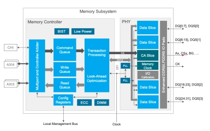
DDR4 Controller
- Maximizes bus efficiency via look-ahead command processing, bank management, auto-precharge and additive latency support
- Latency minimized via parameterized pipelining
- Achieves high clock rates with minimal routing constraints
- Supports half-rate and quarter-rate clock operation
- Supports DDR4 SDRAM 3DS device configurations
-
DDR4/3, LPDDR5x/5/4x/4 Memory Controller IP
- Compliant with JEDEC standard for LPDDR5/4/3, DDR4/3
- DRAM rank of up to 4
- Lock-step-based controlling of multiple DRAM devices up to x64 DQ width
- Support for dynamic DRAM frequency scaling

-
LPDDR4/3, DDR4/3 Memory Controller IP
- Compliant with JEDEC standards for LPDDR4/3, DDR4/3
- DRAM rank of up to 4
- Lock-step-based controlling of multiple DRAM devices up to x64 DQ width
- Support for dynamic DRAM frequency scaling
-
DDR PHY
- DDR5/4/3 training with write-leveling and data-eye training
- Optional clock gating available for low-power control
- Internal and external datapath loop-back modes
- I/O pads with impedance calibration logic and data retention capability
- Programmable per-bit (PVT compensated) deskew on read and write datapaths
- RX and TX equalization for heavily loaded systems
-
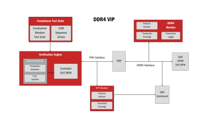
DDR4 Controller - Validates memory compliance, optimizes performance, ensures reliability
- The DDR4 Memory Controller Verification IP ensures compliance with DDR4 standards, validating high-speed data transfer, read/write operations, and error correction. It provides automated testing, advanced debugging tools, and scalability for complex memory systems.
- Designed for versatile applications, this IP optimizes performance in gaming consoles, data centers, AI systems, networking devices, and more. It ensures memory reliability, efficiency, and scalability across industries, accelerating time-to-market for DDR4-based products
-
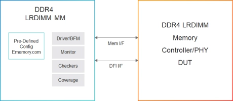
Simulation VIP for DDR4 LRDIMM
- DIMM Types
- DDR4 UDIMM, RDIMM, LRDIMM, DDR4 3DS, 3DS UDIMM, 3DS RDIMM, and 3DS LRDIMM
- LRDIMM Training Modes
- Fully supports DWL, HWL, MREP, MRD, and MWD Training modes
-
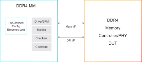
Simulation VIP for DDR4
- Data Width, Density
- 4, 8, and 16. 2 Gb to 16 Gb
- Speed
- 1600, 1866, 2133, 2400, 2666, and 3200
-
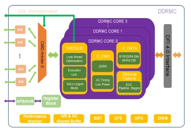
DDR4 IP solution
- Compatible with DDR4 up to 3200Mbps
- AXI compliant multi-ports, and data width, FIFO depth, command queue depth configurable
- DFI compliant interface between controller and PHY
- Support ECC (error correcting code)
-
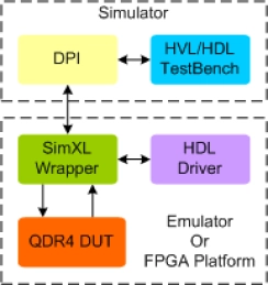
QDR4 Synthesizable Transactor
- Supports 100% of QDR4 protocol standard CY7C4142KV13
- Supports 144-Mbit density (8M × 18, 4M × 36)
- Supports eight-bank architecture enables one access per bank per cycle
- Supports two-word burst on all accesses
-
GDDR4 Synthesizable Transactor
- Supports 100% of GDDR4 protocol standard GDDR4Spec rev 04
- Supports all the GDDR4 commands as per the specs
- Supports all types of timing and protocol violation detection
- Supports all mode registers programming