LPDDR5 Controller IP
Welcome to the ultimate LPDDR5 Controller IP hub! Explore our vast directory of LPDDR5 Controller IP
All offers in
LPDDR5 Controller IP
Filter
Compare
27
LPDDR5 Controller IP
from 8 vendors
(1
-
10)
-
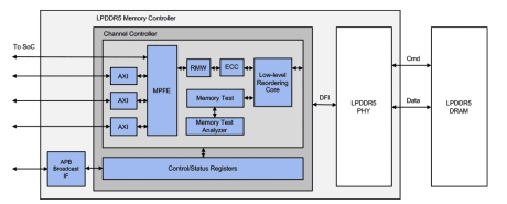
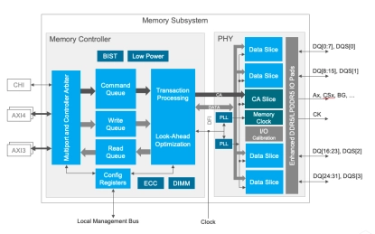
LPDDR5T / LPDDR5X / LPDDR5 Controller
- Support for all LPDDR5T/5X/5 devices
- Bank management logic monitors status of each bank
- Queue-based user interface with reordering scheduler
- Look-ahead activate, precharge, and auto-precharge logic
- Parity protection for all stored control registers
- PHY interface based on DFI 5.1 standard
-
LPDDR5X DDR Memory Controller
- JEDEC LPDDR5X/LPDDR5 devices compatible
- Data rates up to 8533Mbps
- Multiple ARM AMBA AXI4/AHB/APB & Custom interfaces
-
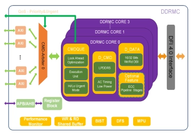
DDR4/3, LPDDR5x/5/4x/4 Memory Controller IP
- Compliant with JEDEC standard for LPDDR5/4/3, DDR4/3
- DRAM rank of up to 4
- Lock-step-based controlling of multiple DRAM devices up to x64 DQ width
- Support for dynamic DRAM frequency scaling

-
LPDDR5X/5/4X/4 Memory Controller IP
- Intensive DRAM Utilization
- Ultra Low Power Consumption
- Extremely Low Latency
- Safety & Security
-
DDR/LPDDR Controller
- Sideband and in-line SEC/DED ECC
- Supports advanced RAS features including error scrubbing, parity, etc.
- Compliant to LPDDR5/4X/4/3 and DDR5/4/3 protocol memories
- Memory controller interface complies with DFI standards up to version 5.0
- Priority per command on Arm® AMBA® 4 AXI, AMBA 3 AXI
-
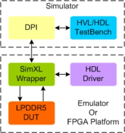
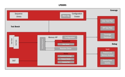
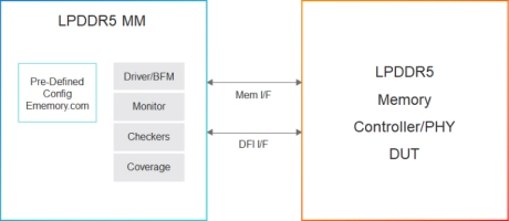
LPDDR5 Controller - Validates memory controllers for high-speed, power-efficient performance
- LPDDR5 Verification IP (VIP) is a tool designed to simulate and validate the functionality of LPDDR5 memory controllers. It ensures compliance with LPDDR5 specifications, covering high-speed data transfer, power management, error detection, and system integration.
- LPDDR5 VIP is essential across various industries, enabling high-performance systems to function optimally. It is utilized in mobile devices, automotive systems, high-performance computing, AI/ML, and more, ensuring efficient memory interfaces in diverse applications
-
Simulation VIP for LPDDR5
- Speed
- 1066.5MHz (8533 Mbps)
- Device Density
- Supports a wide range of device densities from 2Gb to 32Gb
-
LPDDR5 IP solution
- Support LPDDR5 up to 6400Mbps
- Support Channel equalization with 1-tap DFE
- Support single-ended mode on CK, WCK and read DQS below 3200Mbps
- Support Link ECC for RDQS and DM
-
LPDDR5X Synthesizable Transactor
- Supports 100% of LPDDR5X protocol draft JEDEC specification and JESD209-5B specification.
- Supports all the LPDDR5X commands as per the specs.
- Supports device density up to 32GB.
- Supports X8 and X16 device modes.

-
LPDDR5 Synthesizable Transactor
- Supports 100% of LPDDR5 protocol standard JESD209-5, JESD209-5A and JESD209-5B.
- Supports all the LPDDR5 commands as per the specs
- Supports device density up to 32GB
- Supports X8 and X16 device modes