Memory Interface IP for Samsung
Welcome to the ultimate Memory Interface IP for Samsung hub! Explore our vast directory of Memory Interface IP for Samsung
All offers in
Memory Interface IP
for Samsung
Filter
Compare
51
Memory Interface IP
for Samsung
from 5 vendors
(1
-
10)
-
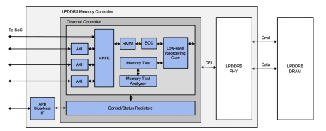
LPDDR5T / LPDDR5X / LPDDR5 Controller
- Support for all LPDDR5T/5X/5 devices
- Bank management logic monitors status of each bank
- Queue-based user interface with reordering scheduler
- Look-ahead activate, precharge, and auto-precharge logic
- Parity protection for all stored control registers
- PHY interface based on DFI 5.1 standard
-
LPDDR5X/5/4X/4 combo PHY at Samsung SF5A
- Compliant for JEDEC standards for LPDDR5X/5/4X/4 with PHY standards
- DFI 5.1 specification PHY Interface Compliant
- Support up to 4 ranks
- x16 and x32 channel support
-
LPDDR5/4x/4 PHY IP for Samsung 14LPU
- Compliant with PHY standards
- Flexible Configuration
- Maximum data rates
-
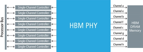
HBM2E/HBM2 PHY
- Advanced clocking architecture minimizes clock jitter
- DFI PHY Independent Mode for initialization and training
- IEEE 1500 interface, Memory BIST feature, and loop-back function
- Designed for optimized interposer routing
- Pin programmable support for lane repair
-
DDR5/4 PHY for Samsung
- Lowest latency for data-intensive applications
- Highest data rates with detailed system guidelines
-
Samsung 8LPU 3.3V SD/eMMC PHY
- Compliant with eMMC 5.1 HS400, SD 6.0 SDR104, DDR50, JESD8-7a (1.2V/1.8V) and JESD8c.01 (3.3V)
- Fully integrated hard macro with high speed IOs and DLL/delay lines
- Fine resolution DLL/delay lines for HS400 strobe and HS200/SDR104 auto-tuning
- Easy to integrate with the highly optimized Synopsys SD/eMMC Host Controller IP, providing a complete low risk solution
-
DDR4 multiPHY SP - SS 14LPP
- Support for JEDEC standard DDR4, DDR3, LPDDR2, and LPDDR3 SDRAMs
- Scalable architecture that supports data rates up to DDR4-2667
- Support for DIMMs
- Delivery of product as a hardened mixed-signal macrocell component allows precise control of timing critical delay and skew paths

-
LPDDR4 multiPHY V2 - SS 8LPU
- Supports JEDEC standard LPDDR4X, LPDDR4, LPDDR3, DDR4, DDR3, and DDR3L (1.35V DDR3) SDRAMs
- Support for data rates up to 4,267 Mbps (process dependent)
- Designed for rapid integration with Synopsys Enhanced Universal DDR Memory/Protocol Controllers (uMCTL2/uPCTL2) for a complete DDR interface solution
- PHY independent, firmware-based training using an embedded calibration processor

-
LPDDR4 multiPHY V2 - SS 8LPP for Automotive AEC-Q100 Grade 1
- Supports JEDEC standard LPDDR4X, LPDDR4, LPDDR3, DDR4, DDR3, and DDR3L (1.35V DDR3) SDRAMs
- Support for data rates up to 4,267 Mbps (process dependent)
- Designed for rapid integration with Synopsys Enhanced Universal DDR Memory/Protocol Controllers (uMCTL2/uPCTL2) for a complete DDR interface solution
- PHY independent, firmware-based training using an embedded calibration processor

-
LPDDR4 multiPHY V2 - SS 8LPP
- Supports JEDEC standard LPDDR4X, LPDDR4, LPDDR3, DDR4, DDR3, and DDR3L (1.35V DDR3) SDRAMs
- Support for data rates up to 4,267 Mbps (process dependent)
- Designed for rapid integration with Synopsys Enhanced Universal DDR Memory/Protocol Controllers (uMCTL2/uPCTL2) for a complete DDR interface solution
- PHY independent, firmware-based training using an embedded calibration processor
