M-LVDS IP
Filter
Compare
470
IP
from 60 vendors
(1
-
10)
-
1.8V/3.3V GPIO Library with HDMI, Aanlog & LVDS Cells in TSMC 22nm
- A TSMC 22nm Inline, Flip Chip compatible library with GPIO, ODIO, HDMI, LVDS, & Analog Cells.
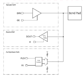
- This silicon-proven, flip chip compatible library in TSMC 22nm boasts a two speed GPIO: 75MHz and 150MHz.
- The library also features a 5V ODIO. GPIO and ODIO cells have an orientation of NS and EW.
-
LVDS Transceiver in TSMC 28nm
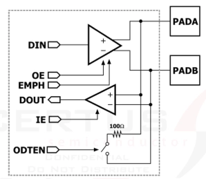
- This 1.8V LVDS transceiver, designed for TSMCs 28nm process, delivers high-speed, low-power differential signaling with superior signal integrity.
- Engineered with 1.8V thick oxide devices and a 0.8V standard core interface, it operates ef- ficiently across a wide temperature range (-40°C to 125°C).
-
GF12 - 0.8V LVDS Rad-Hard Transceiver in GF 12nm
- The 2.5Gbps LVDS transceiver in GlobalFoundries LP/LP+ is designed for high-speed, low-power data transmission in radiation-intensive environments.
- Engineered with a Rad-Hard by Design approach, the Rad-Hard cells have been proton tested to 64 MeV with a flux exceeding 1.3E+09, and is latch-up proven to 200mA across -40C to 125C, ensuring robust immunity against TID, SEE, and SEL effects.
-
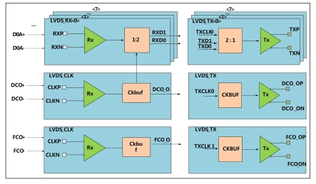
High-speed LVDS (Low-Voltage Differential Signaling) transceiver
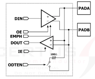
- Compatible with ANSI/TIA/EIA 644-1995 LVDS standard
- Multi-channel LVDS transceiver function
- Maximum data transfer rate: 992Mbps (496MHz)
- Typical output voltage: 350mV (100-Ω load)
-
LVDS Transceiver
- Meets or exceeds the TIA/EIA-644 LVDS standard.
- Driver, Receiver, Bias, and Power cells included.
- Greater than 400Mbs data rate.
- 1.8V core voltage, 3.3V IO voltage.
- Receive fault detection.

-
Open LVDS Display Interface (OpenLDI) Verification IP
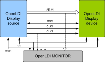
- Full OpenLDI Display Source and Display Device functionality.
- Supports OpenLDI v0.95 specification
- Supports 8 serial data lines (A0 through A7) and two clock lines (CLK1 and CLK2) in the OpenLDI interface.
- Supports DDC2B protocol to retrieve the EDID data structure from display.
-
LVDS Verification IP
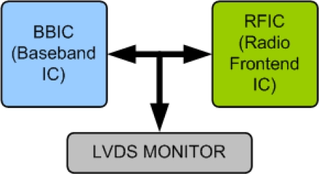
- Follows LVDS Atmel-42415-WIRELESS-AT86RF215_Datasheet specification.
- Supports BBIC and RFIC Mode.
- Supports half duplex data transfer.
- Supports both data path transaction and SPI control interface transactions.
-
LVDS Synthesizable Transactor
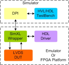
- Follows LVDS Atmel-42415-WIRELESS-AT86RF215_Datasheet specification
- Supports BBIC and RFIC Mode
- Supports half duplex data transfer
- Supports both data path transaction and SPI control interface transactions
-
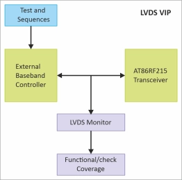
LVDS Verification IP
- Compliant with LVDS Atmel-42415-WIRELESS-AT86RF215_ Datasheet specification.
- Supports dual independent RFIC and respective BBIC.
- Supports serial I/Q LVDS interface.
- Supports SPI control interface.
-
LVDS and OpenLDI PHY
- Silicon proven with maximum speed @1.5Gbps per lane
- Suitable for Automotive applications with ESD levels: HBM > 4KV and CDM > 750V
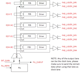
- LVDS TX PHY: 4-data lanes plus 1-clock lane with each lane can be individually turned off
- Supports long-distance transmission: Capable of maintaining signal integrity over longer cable length
