Memory Interface IP for TSMC
Welcome to the ultimate Memory Interface IP for TSMC hub! Explore our vast directory of Memory Interface IP for TSMC
All offers in
Memory Interface IP
for TSMC
Filter
Compare
532
Memory Interface IP
for TSMC
from 18 vendors
(1
-
10)
-
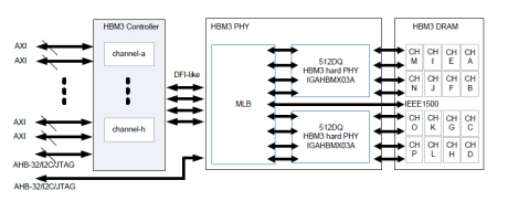
TSMC CLN7FF HBM3 PHY
- IGAHBMX03A is a HBM3 (High Bandwidth Memory) PHY IP compliant to the JEDEC HBM3 DRAM Specification Rev 0.95.
- Built on TSMC 7nm process node, it supports data rate up to 7200 Mbps per data pin with DFI 1:4 clock frequency ratio (controller clock : WCK = 1:4).
-
TSMC N3P 1.8V IO Platform supporting cells
- Compliant with eMMC 5.1 HS400, SD 6.0 SDR104, DDR50, JESD8-7a (1.2V/1.8V) and JESD8c.01 (3.3V)
- Fully integrated hard macro with high speed IOs and DLL/delay lines
- Fine resolution DLL/delay lines for HS400 strobe and HS200/SDR104 auto-tuning
- Easy to integrate with the highly optimized Synopsys SD/eMMC Host Controller IP, providing a complete low risk solution
-
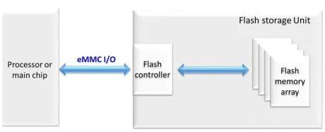
M31 eMMC/SDIO at TSMC 28HPC+ Process
- Supports HS400 (400Mbps), HS200 (200Mbps), High-speed DDR (52Mbps) and etc.
- Consisting of driver, receiver & pull-up/down resistors
- Power-sequence free
- Provides multi-driving-strength selection
-
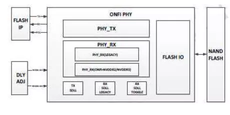
ONFi PHY 4.0 (FPHY+MDLL+SDLL Regulator) (Silicon Proven in TSMC 28HPC+)
- Support ONFi 4.0 IO Electrical Specification
- Support Legacy up to 50MHz
- Support NV-DDR2 with operating frequency up to 533Mbps
- Support NV-DDR3 with operating frequency up to 800Mbps
-
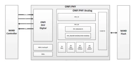
ONFI 4.1 PHY IP (Silicon Proven in TSMC 12FFC)
- Support ONFi 4.1 IO Electrical Specification
- Support Legacy up to 50MHz
- Support NV-DDR2 up to 533Mbps
- Support NV-DDR3 up to 1200Mbps
-
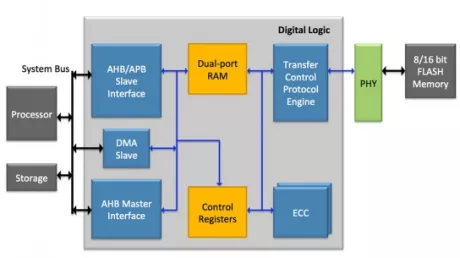
ONFI 4.1 NAND Flash Controller & PHY & IO Pads on 28nm
- Page Size – 2KB, 4KB, 8KB, 16KB
- Bank/chip select options
- Programmable timing

-
ONFI 4.1 NAND Flash Controller & PHY & IO Pads on 16nm
- Page Size – 2KB, 4KB, 8KB, 16KB
- Bank/chip select options
- Programmable timing
-
ONFI 4.1 NAND Flash Controller & PHY & IO Pads on 12nm
- Page Size – 2KB, 4KB, 8KB, 16KB
- Bank/chip select options

-
GDDR6 PHY
- Single configuration supports one GDDR6 device per channel (coplanar) or two GDDR6 devices per channel (clamshell)
- DFI PHY Independent Mode for initialization and training
- Adaptive and continuous timing recovery
- Internal and external datapath loop-back modes
- Transmit crosstalk cancelation of immediate neighbors
- Per-bit DFE, CTLE, and FFE equalization
-
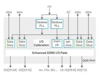
DDR5/4 PHY for TSMC 7nm
- Application optimized configurations for fast time to delivery and lower risk
- Memory controller interface complies with DFI standards up to 5.0
- Internal and external datapath loop-back modes
- Per-bit deskew on read and write datapath