Key attributes of the 130nm IO library include an extended operational temperature range (-55°C to 200°C), sleep retention, and a built-in power regulation PMOS device for core VDD. The GPIO cell can be configured as input, output or open-drain with an optional internal 60K ohm pull-up or pull-down resistor and a selectable Schmitt trigger. ESD protection for IO and core supplies is constructed in an aggressive footprint. 3.3V LVDS TX & RX cells, along with 3.3V OTP programming, 3.3V I2C open drain and analog cells complement the GPIO offering. The library is enriched with feed-through, filler, corner and domain-break cells to allow for flexible pad ring construction.
Built into our IO libraries, and also offered as a separate service, is our strong ESD expertise. Certus was founded by ESD engineers and our results speak for themselves. Not only do we consistently exceed the standard ESD targets of 2KV HBM and 500V CDM, but we also provide on-chip solutions for standards such as IEC-61000-4-2, system-level ESD and Cable Discharge Events (CDE).
Certus supports IO libraries across multiple TSMC nodes including 180nm, 130nm, 40nm, 28nm, 22nm, and 16/12nm. Certus is particularly suited at providing custom variants in a cost-efficient framework. Please contact us for supplementary physical or electrical features that can suit your needs.
A 130nm Wirebond IO library with 3.3V GPIO, LVDS TX & RX, 3.3V I2C open-drain, analog cell and OTP program cell
Overview
Key Features
- GPIO:
- Extended operational temperature range (-55°C to 200°C)
- Sleep retention
- Built-in regulation PMOS device for VDD supply
- Independent output and input enable / disable
- Selectable Schmitt trigger receiver
- Selectable 60K? pull-up or pull-down resistor
- ESD: 2KV HBM, 500V CDM
- Silicon proven
- I2C / SMBUS Open-Drain I/O:
- Up to 3.3V external supply support
- Hysteresis input
- Power sequence independence
- External resistor support of 1K-50K Ohm
- Fail-safe
- 2KV HBM, 500V CDM
- Also DDC, CEC and HPD compliant
- LVDS
- Receive and transmit two-pad cells
- Output & Input enable
- Built-in 100? RX termination resistor
- Fail-safe mode for shorted or open RX pins
- Internally generated common mode reference (no external pin required)
- Power-on sequence independence
- ESD protection of 2KV HBM, 500V CDM
- ANALOG
- 3.3V tolerant
- 2KV HBM, 500V CDM
- OTP Programming Cell
- 3.3V tolerant supply gating cell
- 2KV HBM, 500V CDM
- Physical Attributes
- 8-metal stack - 6X1Z
- 140um x 235um cell size
- 140um single inline wirebond pitch
Benefits
- Extended operational range (-55°C to 200°C)
- Sleep retention
- Built-in regulation PMOS for VDD supply
- Pull-up / pull-down resistor options
- 3.3V LVDS RX & TX cells (150-200 MHz)
- 3.3V I2C open-drain & analog cells
- 140um single inline wirebond pitch
- Silicon proven
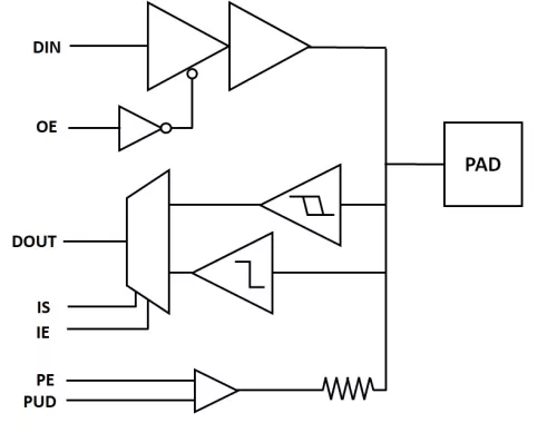
Block Diagram
Applications
- LVCMOS, GPIO, I2C, SVID, DDC, CEC, HPD, LVDS, OTP, Analog
Deliverables
- GDS
- CDL netlist
- Verilog stub
- Verilog behavioral model
- LEF
- Liberty Timing Files
- IBIS (optional)
- Electrical datasheet
- User guide and application notes
- Consulting and Support
Technical Specifications
Foundry, Node
TSMC 130nm
Maturity
Silicon-Proven
Availability
Immediate
TSMC
In Production:
130nm
G
,
130nm
LP
Pre-Silicon: 12nm , 130nm G , 130nm LP
Silicon Proven: 130nm G , 130nm LP
Pre-Silicon: 12nm , 130nm G , 130nm LP
Silicon Proven: 130nm G , 130nm LP
Related IPs
- 28nm Wirebond IO library with dynamically switchable 1.8V/ 3.3V GPIO, 5V I2C open-drain, 1.8V & 3.3V analog, OTP program cell, and HDMI & LVDS protection macros - featured across a variety of metal stack and pad configuration options
- A 65nm Wirebond IO library with 1-3.3V GPIO, 3.3V pulse-width modulation cell, I2C & SVID open-drain, 3.3V & 5V analog and OTP program cell
- A 180nm Flip-Chip IO library with 1.2-1.8V GPIO, 1.8V & 5V analog/RF, 20-36V ultra-low leakage low-cap HV analog and OTP program cell
- CSMC 0.13um 3.3V Standard Cell Library, 3.3v operating voltage
- 1.8V/3.3V Switchable GPIO With 3.3V I2C Open Drain & Analog in 22nm
- A 65nm Wirebond IO library with 2.5V GPIO, LVDS TX & RX and 2.5V analog / RF