DDR2 PHY IP
Welcome to the ultimate DDR2 PHY IP hub! Explore our vast directory of DDR2 PHY IP
All offers in
DDR2 PHY IP
Filter
Compare
6
DDR2 PHY IP
from 4 vendors
(1
-
6)
-
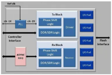
ONFI 3.2 NV-DDR2 PHY in GDSII
- Compliant to ONFI revision 3.2 standard
- Supports NV-DDR2 mode of operation supporting up to 266MHz or 566MT/s
- Supports NV-DDR mode of operation supporting up to 100MHz
- Supports legacy Asynchronous devices operating from 10MHz to 50MHz
-
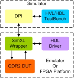
QDR2 Synthesizable Transactor
- Supports 100% of QDR2 protocol standard CY7C1314CV18
- Supports separate independent read and write data ports with concurrent read and write operation
- Supports full data coherency, providing most current data
- Supports synchronous pipeline read with self-timed late write
-
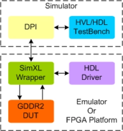
GDDR2 Synthesizable Transactor
- Supports 100% of GDDR2 protocol standard
- Supports all the GDDR2 commands as per the specs
- Supports all types of timing and protocol violation detection
- Supports all mode registers programming
-
Gen 2 DDR multiPHY IP
- Support for JEDEC standard LPDDR2, LPDDR3, and DDR3 SDRAMs
- Scalable architecture that supports data rates up to DDR3-2133
- Support for DIMMs
- Delivery of product as a hardened mixed-signal macrocell components allows precise control of timing critical delay and skew paths

-
DDR3/2 PHY - TSMC 40LP25
- When combined with a Synopsys DDR memory or protocol controller and verification IP, Synopsys provides a complete DDR3/2 interface IP solution
- Scalable architecture that supports the speed range from DDR2-667 up to DDR3-2133
- Support for DDR3L (1.35V DDR3)
- Support for DDR2 and DDR3 DIMMs

-
LPDDR PHY
- Application-optimized configurations for fast time to delivery and lower risk
- Low-power VDD idle, VDD light sleep, and power-efficient clocking in low-speed modes
- I/O pads with impedance calibration logic and data-retention capability
- Fine-grain custom delay cell for delay tuning
- Internal and external datapath loop-back modes
- RX and TX equalization for heavily loaded systems
- Programmable per-bit (PVT compensated) deskew on read and write datapaths