USB IP for SMIC
Welcome to the ultimate USB IP for SMIC hub! Explore our vast directory of USB IP for SMIC
All offers in
USB IP
for SMIC
Filter
Compare
52
USB IP
for SMIC
from 10 vendors
(1
-
10)
-
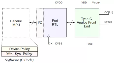
Complete USB Type-C Power Delivery IP
- Mixed signal Analog Front End Macros for 65n, 130n, 150nm, and 180n technologies.
- RTL code from AFE to I2C compatible register set.
- Stand alone C code for Protocol, Device Policy Manager, and System Policy Manager.
- IP demonstration & development board, with compliance reports.
- Full chip integration of USB Type-C, and associated software.
-
USB 2.0 femtoPHY - SMIC 28PS18 x1, North/South (vertical) poly orientation
- Ported to over 50 different processes and configurations ranging from 65-nm to 14/16-nm FinFET
- Supports the USB 2.0 protocol and data rate (480 Mbps)
- Supports the USB Type-C specification
- USB femtoPHY, USB nanoPHY and USB picoPHY offer a tunability feature that allows quick, post-silicon adjustments that occur due to process variations, or unexpected chip and board parasitic, without modifying the existing design

-
USB 2.0 femtoPHY - SMIC 28HKMG18 x1, OTG, North/South (vertical) poly orientation
- Ported to over 50 different processes and configurations ranging from 65-nm to 14/16-nm FinFET
- Supports the USB 2.0 protocol and data rate (480 Mbps)
- Supports the USB Type-C specification
- USB femtoPHY, USB nanoPHY and USB picoPHY offer a tunability feature that allows quick, post-silicon adjustments that occur due to process variations, or unexpected chip and board parasitic, without modifying the existing design
-
USB1.1 build-in clock PHY, SMIC 55LL
- Smallest USB 3.2 Gen1x1 BCK PHY IP worldwide (e.g. IP size @40nm <0.36mm²)
- Fully compliant with Universal Serial Bus USB 3.2 Gen1x1, 2.0, and 1.1 electrical specifications
- Supports clock outputs from the internal BCK module
- Real-time calibrations to ensure frequency accuracy

-
USB2.0 build-in clock PHY, SMIC 55LL
- Smallest USB 3.2 Gen1x1 BCK PHY IP worldwide (e.g. IP size @40nm <0.36mm²)
- Fully compliant with Universal Serial Bus USB 3.2 Gen1x1, 2.0, and 1.1 electrical specifications
- Supports clock outputs from the internal BCK module
- Real-time calibrations to ensure frequency accuracy
-
USB2.0 build-in clock PHY, SMIC 40LL, type-C
- Smallest USB 3.2 Gen1x1 BCK PHY IP worldwide (e.g. IP size @40nm <0.36mm²)
- Fully compliant with Universal Serial Bus USB 3.2 Gen1x1, 2.0, and 1.1 electrical specifications
- Supports clock outputs from the internal BCK module
- Real-time calibrations to ensure frequency accuracy

-
USB3.0 build-in clock PHY, SMIC 55LL
- Smallest USB 3.2 Gen1x1 BCK PHY IP worldwide (e.g. IP size @40nm <0.36mm²)
- Fully compliant with Universal Serial Bus USB 3.2 Gen1x1, 2.0, and 1.1 electrical specifications
- Supports clock outputs from the internal BCK module
- Real-time calibrations to ensure frequency accuracy

-
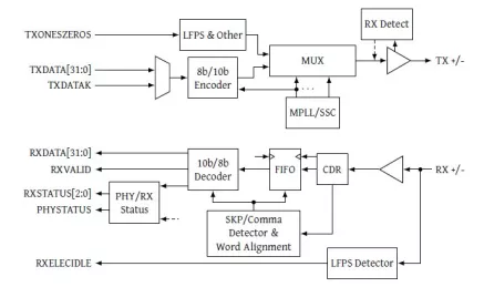
USB 3.0 PHY
- Standard PHY interface (PIPE) enables multiple IP sources for USB 3.0 Link Layer
- Supports 5.0 GT=s serial data transmission rate
- Supports 16- or 32-bit parallel interface
- Supports PCLK as PHY output
-
CSMC 0.13um USB 1.1 PHY
- Complies with the USB1.1 standard
- CSMC 0.13um, 1.2v/3.3v power supply, 1P6M logic process
- Uses digital input/output to transmit or receive USB cable data
- Supports 12Mbit/s full speed and 1.5Mbit/s low speed serial data transmission
-
GLOBALFOUNDRIES 28nm USB2.0 Dual Role PHY/OTG PHY
- Compliant with the USB Spec Rev2.0
- Compliant with the UTMI Spec Rev1.05/UTMI+ Spec Rev1.0 Level3
- Supports 480Mbit/s "High Speed" and 12Mbit/s "Full Speed"
- Supports 60MHz/8-bit unidirectional interface and 30MHz/16-bit bidirectional interface