USB IP for GLOBALFOUNDRIES
Welcome to the ultimate USB IP for GLOBALFOUNDRIES hub! Explore our vast directory of USB IP for GLOBALFOUNDRIES
All offers in
USB IP
for GLOBALFOUNDRIES
Filter
Compare
34
USB IP
for GLOBALFOUNDRIES
from 7 vendors
(1
-
10)
-
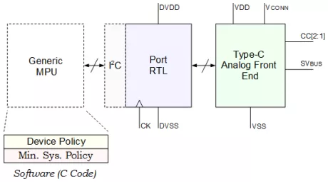
Complete USB Type-C Power Delivery IP
- Mixed signal Analog Front End Macros for 65n, 130n, 150nm, and 180n technologies.
- RTL code from AFE to I2C compatible register set.
- Stand alone C code for Protocol, Device Policy Manager, and System Policy Manager.
- IP demonstration & development board, with compliance reports.
- Full chip integration of USB Type-C, and associated software.
-
USB 2.0 nanoPHY - GF 55LPE25, OTG
- Ported to over 50 different processes and configurations ranging from 65-nm to 14/16-nm FinFET
- Supports the USB 2.0 protocol and data rate (480 Mbps)
- Supports the USB Type-C specification
- USB femtoPHY, USB nanoPHY and USB picoPHY offer a tunability feature that allows quick, post-silicon adjustments that occur due to process variations, or unexpected chip and board parasitic, without modifying the existing design

-
USB 2.0 femtoPHY - GF 28SLP18 x1, OTG, East/West (horizontal) poly orientation
- Ported to over 50 different processes and configurations ranging from 65-nm to 14/16-nm FinFET
- Supports the USB 2.0 protocol and data rate (480 Mbps)
- Supports the USB Type-C specification
- USB femtoPHY, USB nanoPHY and USB picoPHY offer a tunability feature that allows quick, post-silicon adjustments that occur due to process variations, or unexpected chip and board parasitic, without modifying the existing design

-
USB 2.0 picoPHY - GF 28SLP18 x1, East/West poly orientation
- Ported to over 50 different processes and configurations ranging from 65-nm to 14/16-nm FinFET
- Supports the USB 2.0 protocol and data rate (480 Mbps)
- Supports the USB Type-C specification
- USB femtoPHY, USB nanoPHY and USB picoPHY offer a tunability feature that allows quick, post-silicon adjustments that occur due to process variations, or unexpected chip and board parasitic, without modifying the existing design

-
USB 2.0 femtoPHY - GF 22FDSOI18 x1, N/S, for Automotive, ASIL B Random, AEC-Q100 Grade 1
- Ported to over 50 different processes and configurations ranging from 65-nm to 14/16-nm FinFET
- Supports the USB 2.0 protocol and data rate (480 Mbps)
- Supports the USB Type-C specification
- USB femtoPHY, USB nanoPHY and USB picoPHY offer a tunability feature that allows quick, post-silicon adjustments that occur due to process variations, or unexpected chip and board parasitic, without modifying the existing design
-
USB 2.0 femtoPHY - GF 22FDSOI x1, OTG, North/South (vertical) poly orientation
- Ported to over 50 different processes and configurations ranging from 65-nm to 14/16-nm FinFET
- Supports the USB 2.0 protocol and data rate (480 Mbps)
- Supports the USB Type-C specification
- USB femtoPHY, USB nanoPHY and USB picoPHY offer a tunability feature that allows quick, post-silicon adjustments that occur due to process variations, or unexpected chip and board parasitic, without modifying the existing design

-
USB 2.0 femtoPHY - GF 12LPP18 x1, OTG, North/South (vertical) poly orientation
- Ported to over 50 different processes and configurations ranging from 65-nm to 14/16-nm FinFET
- Supports the USB 2.0 protocol and data rate (480 Mbps)
- Supports the USB Type-C specification
- USB femtoPHY, USB nanoPHY and USB picoPHY offer a tunability feature that allows quick, post-silicon adjustments that occur due to process variations, or unexpected chip and board parasitic, without modifying the existing design

-
USB 2.0 femtoPHY - GF 12LP x1, OTG, North/South (vertical) poly orientation
- Ported to over 50 different processes and configurations ranging from 65-nm to 14/16-nm FinFET
- Supports the USB 2.0 protocol and data rate (480 Mbps)
- Supports the USB Type-C specification
- USB femtoPHY, USB nanoPHY and USB picoPHY offer a tunability feature that allows quick, post-silicon adjustments that occur due to process variations, or unexpected chip and board parasitic, without modifying the existing design

-
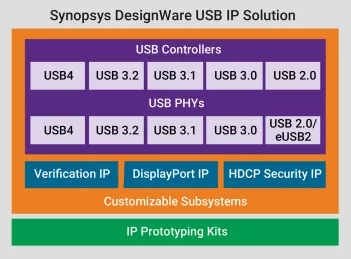
USB-C 3.2 DP/TX PHY for GF 12LP+, North/South poly orientation
- USB-IF certified Synopsys USB 3.2 solution
- VESA certified Synopsys DisplayPort 1.4 Tx solution
- Industry’s only USB Type-C IP solution consisting of USB-C 3.2/DisplayPort 1.4 TX PHYs, USB-C 3.2/DisplayPort 1.4 TX controllers with HDCP 2.2 and HDCP 2.2 content protection, verification IP, and IP subsystems
- Solution supports USB Type-C, SuperSpeed USB 3.2 at 20 Gbps, SuperSpeed USB 3.1 at 10 Gbps, SuperSpeed USB 3.0 at 5 Gbps and High-Speed USB (USB 2.0) as well as DisplayPort 1.4 TX supporting RBR, HBR1, HBR2 and HBR3 bitrates

-
USB 3.1 PHY (10G/5G) - GF 22FD-SOI x1, North/South Poly Orientation
- Part of a complete IP solution including xHCI host and device controllers, PHYs, verification IP, 1 IP Prototyping Kits and IP software development kits
- Designed for advanced 1.8V CMOS planar bulk and FinFET process nodes
- USB-C 3.1 PHY IP supports USB Type-C specification
- Supports the SuperSpeedPlus (10 Gbps) and SuperSpeed (5 Gbps) speed modes
