Gigacom's VSL340A PHY updated version of VSL340 to support SATA3 and backward compatible with SATA 1 and 2. VSL340A is suitable for both Host and Device applications within a Serial ATA system. The VSL340A PHY operates to the Serial ATA specification using either a 10-bit or 20-bit interface to a Serial ATA Link Layer where the 8b10b encoding and decoding of the data is done. Recovered data is provided using SATA compliant D-word alignment. The VSL340A PHY provides a comprehensive feature set, a well-defined architecture that allows designers extensive flexibility for various applications, and a roadmap to future products.
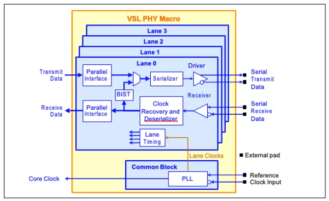
The VSL340A PHY is comprised of a hardened GDSII Physical Medium Attachment (PMA) sublayer containing the SerDes, plus a soft Physical Coding Sublayer (PCS) Verilog module that is connected to the hard macro at the PMA interface. The PCS, when coupled with the hardened PMA SerDes macro, provides a Serial ATA PHY with compliant signals for the end customer. Since the VSL PHY family includes many test features and capabilities that are not part of the Serial ATA specification, additional pins from the PMA layer are also available.
SATA 3 PHY
Overview
Key Features
- Serial ATA III Revision 3.3 compliant
- Gen1i, Gen1m, Gen2i, Gen2m compliant
- Gen1x, Gen2x compatible
- Initialization and power saving modes
- Full ±5700 ppm data tracking capability in all modes (with elastic buffer build option)
- Transmission jitter generation and receiver jitter tolerance which exceed Serial ATA jitter specifications
- 10 or 20 bit interface (build option)
- Serial ATA compliant command and status signals
- K28.5 comma detection
- ALIGN detection and alignment
- Selectable lane polarity inversion
- Host or Device applications
- Programmable serial transmit amplitude
Benefits
- Low Risk - Silicon proven today in multiple foundries and processes with Extensive Si characterization data
- Excellent Interoperability – Both LC tank and Ring oscillator options based on process node to gives low noise and jitter
- Superior Noise Immunity - Fully differential circuitry and Voltage Regulator for enhanced noise immunity
- Low Power – Contact us for the details for your process node
- Minimal Area - for Wire bond as well as flip-chip package
- Improve Test Coverage - Multiple loopback modes with 12 built-in patterns
- Scan built in to all digital,Serial Control Register (SCR) for simplified testing, JTAG support (DC and AC )
- Lowest Total Cost of Ownership
- Customization/ Integration support
Block Diagram

Applications
- Hard drive interfaces
Deliverables
- Abstract - LEF
- Behavioral Model -Verilog
- Timing Model -.lib
- High-speed IO Model - hSpice
- LVS Netlist - cdl
- Physical database - GDSII
- Documentation - pdf
Technical Specifications
Foundry, Node
TSMC 65nm, Globalfoundries 40nm, Globalfoundries 55nm, Silicon proven in TSMC 28nm HPC/HPC+
Maturity
Production proven
Availability
TSMC 65nm, GF 55nm, GF 14nm, GF 22nm, Silicon proven in TSMC 28nm HPC/HPC+