The Sofics 1.8V capable GPIO is an IP macro for on-chip integration. It is a 1.8V general purpose I/O built with a stack of 1.2V MOS FINFET devices. It is controlled by 0.75V (core) signals.
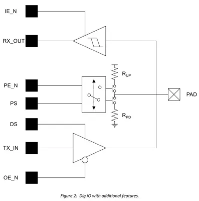
Supported features include core isolation, output enable and pull enable.
Extra features such as input enable/disable, programmable drive strength and pull select, can be supported upon request.
By default, a 2kV HBM ESD protection is included. This is however easily scaled to any desired level.
This specific IP macro is designed in Samsung 4nm FINFET, and can be ported to other technologies upon request using Sofics inhouse design tool flow
1.8V general purpose I/O for 4nm FinFET
Overview
Key Features
- Functional I/O circuit and ESD protection cells
- Enable higher voltage tolerance, beyond foundry I/O voltage levels
- Overvoltage tolerant design
- DFM rules for manufacturing
- Core domain isolation
- Compatible with TSMC I/O ring
- Temp range -40°C to 125°C TJ
- 50k? pullup/pulldown
- Integrated 2kV HBM ESD
- 0.75V digital interface at the core side
- Bias generation circuit can be shared over multiple I/O instances
Benefits
- Enable higher voltage operation, beyond the foundry IO levels
- Easily replace existing I/O cells
- Integrated scalable ESD protection
- Bias circuit can be shared with multiple I/Os
- Options
- Input enable/disable
- programmable drive strength
- pull select
Block Diagram
Applications
- Every IC design that requires a higher/lower voltage tolerance
Deliverables
- GDSII
- LVS support
- Datasheet
- Documentation
- Integration guidelines and services
Technical Specifications
Foundry, Node
All foundries and processes
Maturity
Silicon proven
Availability
Immediate
Samsung
Silicon Proven:
4nm