Functional Verification of a CAN data layer implementation: a case study
Brazil Semiconductor Technology Center (BSTC) – SPS – Motorola
Jaguariúna - Brazil
Abstract
A new verification strategy used to validate an IP implementing the CAN protocol is introduced. The proposed strategy is a result of the analysis of the pros and cons of some known methodologies, whose aspects are presented. By adopting this approach, the verification cycle was considerably reduced, as will be seen by comparative data to be presented. The testbench is built up from the C reference model provided by BOSCH and a user defined set of drivers and monitors written in C++, using Testbuilder as a basis.
1. Introduction
The Controller Area Network (CAN) is a serial communication protocol with transfer rates up to 1Mbit/s[1]. It has multi-master capabilities and its messages are content-addressed , which means that a message is broadcast to all nodes (including the transmitter itself), and each node decides whether the message should be received or discarded.
Its powerful error detection properties combined with a fault confinement operation based on statistic analysis, which can even disconnect the node from the network, allows its use in critical automotive applications such as ABS controllers, although we may found CAN transceivers in a wide range of applications ranging from medical equipment to domestic appliances[2].
This wide range of applications has attracted several major chip manufacturers. Moreover, a quick search on the internet reveals that there are more than 20 IP-vendors which provide CAN cores for embedded applications[3].
When it comes to functional verification, two aspects should be considered:
- Since market requirements tend to evolve, such an IP is prone to changes, and the effort necessary to verify enhanced versions of the module depends on the reusability of the verification environment.
- The infrastructure used to validate the design at the module level (standalone verification) may be reused to facilitate the SoC verification, whose main focus is the correct integration of the module.
In this paper we describe the Functional Verification of a CAN Data Link Layer Implementation that succeeded in addressing those aspects. The verification environment includes a high-level Verilog model converted from the C model provided by BOSCH[4] and a complete infrastructure using TestBuilder[8] as a basis.
The paper is organized as follows: Section 2 presents an overview of the Device Under Verification (DUV): the FlexCAN2 module. In Section 3, we analyze some aspects of commonly used verification methodologies, while in Section 4 we present our verification environment. In Section 5, comparative data is shown for the sake of quantitative evaluation. Finally, our conclusions are expressed in Section 6.
2. Device Under Verification: the FlexCAN2 IP
The FlexCAN2 module is a communication controller implementing the CAN protocol according to the CAN 2.0B protocol specification[1], with the following distinctive features:
- Up to 64 Message Buffers (MB’s), which can be individually configured as TX or RX buffers
- Reception masks for IDENTIFIER (ID) acceptance, used when an RX MB should receive a range of ID’s
- A data coherence mechanism to prevent corruption of information when the CPU is accessing an RX MB that is about to be loaded with another received message
- Two clock domains, to comply with tight jitter requirements: in microcontrollers with internal frequency modulated PLL (to reduce electromagnetic radiation), the clock feeding the CAN engine can be selected to be derived from the oscillator clock instead of the PLL output
- Programmable transmission priority scheme: lowest ID among TX MB’s or lowest TX MB number is transmitted first.
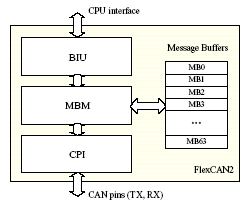
The module is composed of three major blocks as depicted in figure 2.1:

Figure 2.1: the FlexCAN2 module
The CAN Protocol Interface (CPI) sub-module manages the serial communication on the CAN bus, requesting RAM access for receiving and transmitting message frames, validating received messages and performing error handling.
The Message Buffer Management (MBM) submodule handles Message Buffer selection for reception and transmission, taking care of arbitration and ID matching algorithms.
The Bus Interface Unit (BIU) sub-module controls the access to and from the internal 32-bit peripheral bus, in order to establish connection to the CPU and to other blocks. Clocks, address and data buses, interrupt outputs and test signals go through the Bus Interface Unit.
The FlexCAN2 was implemented as a fully synthesizable soft block with approximately 20 thousand equivalent nand2 gates, and it is targeted for high performance 32-bit microcontrollers.
Unlike previous verification efforts devoted to other CAN transceiver IP’s within Motorola, the Verification IP was built to be fully compliant to the Motorola Semiconductors Reuse Standards[5], in order to facilitate the integration of the module into new SoC’s. In our experience, the documentation overhead generally represents from 25 to 30% of the total amount of work.
It is also worth mentioning that in order to reduce the effort needed to verify potential future versions of the module (to include new features), the Verification IP should avoid relying on controlling and/or probing internal state machines or architecture dependent signals, that is, the DUV should be treated as a black box as far as possible. The major goal of this verification strategy was to satisfy the constraints above while enabling a considerable reduction in the functional verification cycle due to resources and schedule constraints.
3. Commonly Used Verification Methodologies
In this section, we analyze several aspects of some verification methodologies commonly used to validate designs targeted for the automotive market. Several different approaches have already been published:
In [6], the verification of an 8-bit microcontroller core was accomplished through the use of directed functional verification patterns. The list of patterns was created from the process known as "Spec Tagging", which consists of associating each functional sentence in the spec to a directed pattern (stimulus vector). The verification patterns are considered self-checking because they contain both the stimuli to be applied to the DUV as well as the expected results to be checked.
Although this method can result in a high functional coverage, it has some drawbacks: besides, depending on the accuracy of the specification, a complex design with large FSM’s (as in the case of communications protocols) would require writing a large number of hand-crafted patterns to check all combinations of states, which is very time-consuming. Generally speaking, corner cases are not explicit in the specifications, and in this case they are left to be covered by the verification engineer’s talent.
In [7], a set of random stimuli is used to validate a microprocessor core. The verification is accomplished by comparing the outputs of the DUV with the outputs of a high-level model, both being stimulated with the same attributes. This method is very common in the verification of high performance microprocessors.
Although very simple in nature (the stimuli generator is derived from a random number generator), the corner cases are generally reached only in long simulation runs. Moreover, in some cases the high-level model is required to be cycleaccurate and implementation-specific, increasing the complexity of the model itself and its validation process.
4. Case Study
The verification strategy consisted of three major actions:
First, the functionality of the design was partitioned into 2 domains: those features to be implemented in a behavioral model and verified through the use of randomization and the features verified through the use of hand-crafted directed patterns, in which only secondary behavior was compared against the model.
The primary challenge was to establish the boundary between those two domains, taking into account the following constraints:
- The behavioral model had to be simple enough to be quickly verified and stable to start running in only 2 months. Nevertheless, it should be meaningful enough to allow automatic free-running check of interrupts, CAN related pins and message buffer contents, in order to reduce the amount of directed patterns required.
- Directed patterns should cover the functionality not implemented in the model as well as verify corner cases in situations like low-power mode requests and changes in the configuration of the MB’s while the module executes transactions in the CAN line.
The criteria used to set the boundary between these two domains was based on a previous evaluation of the efforts required to verify the major functional blocks in each of the two partitions (model or directed patterns). It was also determined that the interrupt flags should be implemented in the model and checked via free-running monitors.
After having partitioned the features, the verification team was divided in two groups, to work concurrently in each of the functional domains.
The only requirement for the model was that it should be cycle-accurate from the CAN pins standpoint. Unless for the Bit Timing Unit (BTI), a tiny part of the model that deals with the timing of the CAN pins, a great non cycle-accurate part of the model was implemented by zero-time tasks and functions, which update state, values of ERROR COUNTERS, contents of an MB, interrupt flags, etc., and are called by events triggered by the BTI machine.
This allowed us to have a stable model up and running in a very short period of time. The same approach was used to implement the drivers of the model: the driver accesses the registers of the model directly, via zero-time tasks.
The second action consisted in implementing a high level Stimulus Interface, that isolated the stimulus writers from the details of the CAN protocol. This was essential to enable part of the team responsible for the creation of the directed tests (who were not CAN experts at the beginning of the project) to quickly become productive. By using the tasks available in the Stimulus Interface, it is possible to apply rather complex stimulus to the DUV with very few task calls.
The last action improved on the methodology used to create the directed pattern suite using “Spec Tagging”. A brainstorm meeting with the entire team was held prior to any code writing, to discuss potential corner cases to be checked. By focusing on corner cases from the very beginning, a great percentage of the total bugs was uncovered in very early phases of the design, quickly raising the level of confidence on it.
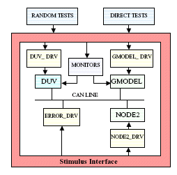
The complete verification environment is depicted in figure 4.1, whose elements will be detailed in the next sub-sections. In this figure, GMODEL and NODE2 are two instances of the behavioral model, and the suffix “_DRV” stands for driver. NODE2 is used to serve as a second CAN node for the purpose of simulating a real CAN network.
The tool of choice to implement the drivers, monitors and stimulus interface was Testbuilder[8]. The patterns are also written in Testbuilder, and are mainly composed of calls to the tasks and functions implemented in the Stimulus Interface

Figure 4.1: the Verification Environment
4.1. The Golden Model
The golden model, hereafter referenced as GMODEL, is composed of two main blocks: a CAN transceiver and a Message Buffer Processing Unit, which implements the MB's, reception masks for ID acceptance, interrupt flags and the algorithm for choosing the next messages to be transmitted. The model was written in Verilog to facilitate debugging and portability, and its CAN transceiver sub-block was manually converted from the C model provided by Bosch[4].
4.2. Drivers
A bus functional model of the peripheral bus was used to access the memory mapped registers of the DUV. All behavioral models in Figure 4.1 are controlled via zero-time tasks, as mentioned earlier.
4.3. Free-Running Monitors
A set of free-running monitors was built to automatically check interrupt generation, changes in the error counters, TX pin state and MB contents.
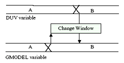
Since a considerable part of the model is not cycleaccurate, a new strategy had to be adopted by the monitors, instead of comparing the outputs of the model with those of the DUV in a cycle-by-cycle basis. The strategy is depicted in figure 4.2:

Figure 4.2: Monitor mechanism
Whenever the GMODEL changes one pertinent variable, the DUV is allowed to update its state (according to the model) within a time window. In our case, the point inside the window at which the DUV actually changes its state was influenced by several variables, and is implementation dependent. It was possible to set a time window that is shorter than the minimum possible time between changes. To prevent spurious transitions in the DUV, whenever it changes a pertinent variable, the variable is compared against that of the model.
4.4.Stimulus Interface
The stimulus interface is composed by a set of tasks that control the drivers of the DUV, GMODEL and NODE2 (another instance of the GMODEL used to serve as a second CAN node for the purpose of simulating a real CAN network), and also the ERROR driver (used to force global or local bit errors in the network).
Through the use of overloading, any omitted arguments in a task call are automatically randomized, greatly reducing the code complexity. The stimuli can control whether the DUV and GMODEL are configured individually or, by default, with the same attributes. They are also able to enable, configure and disable all free-running monitors.
5. Comparative Data
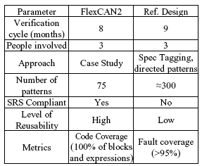
For the sake of quantitative evaluation, Table 5.1 shows comparative data of the verification efforts of FlexCAN2 and one of its predecessors.

Table 5.1: Comparative data
One can see from this table that despite the documentation overhead and the higher complexity of the IP, the verification cycle was reduced.
Another interesting information for comparison is the effort required to reuse the Verification IP of the reference design: to port the verification suite to another platform aiming to verify a slightly modified version of the reference design developed concurrently to FlexCAN2, 3 people got involved during approximately 8 months, the same time we invested to build a reusable environment up from scratch.
Our environment was reused to verify a very recent enhanced version of the FlexCAN2, including new features such as the option of creating queues for received messages, and in only 2 months the design was completely validated.
Moreover, once having a behavioral model written in Verilog, it was just a matter of porting to Verilog some of the tasks of the driver of the GMODEL and Stimulus Interface (a process that took just one person-day) to complete the SoC verification of the FlexCAN2 module in just one week.
6. Conclusions
By balancing the accuracy level of the behavioral model with the amount of hand-crafted directed patterns and having the option to work in a high level of abstraction, it was possible to reduce considerably the verification cycle of a CAN Data Layer Implementation, while achieving a high functional coverage.
As presented in Section 5, the effort necessary to reuse the Verification IP was reduced by a factor of 4, when compared to the reference design. Two requirements of the Verification IP were crucial to enable this: to be fully SRS compliant and to treat the DUV as a gray box.
References
[1] ISO International Standard 11898. Road vehicles - Interchange of digital information - Controller area network (CAN) for high-speed communication, November 1993.
[2] W. Lawrenz. CAN System Engineering – From Theory to Practical Applications. Springer-Verlag, New York, 1997.
[3] Design-Reuse. www.design-reuse.com
[4] Bosch’s Controller Area Network. www.can.bosch.com
[5] Semiconductors Reuse Standards. www.motorola.com Search for “SRS”.
[6] N. Sabbatini Jr et Al, "Reuse Issues on the Verification of Embedded MCU Cores", Proceedings of the Fourth IEEE International Caracas Conference on Devices, Circuits and Systems, April, 2002.
[7] W. S. Encinas Jr. and C. A. Dueñas Moran, "Functional Verification in 8-bit Microcontrollers: A Case Study", XVI International Conference on Microelectronics and Packaging, Pirenópolis, Brazil, Sep 10-14, 2001, pp. 168-73.
[8] Tesbuilder. www.testbuilder.net
Related Semiconductor IP
- Root of Trust (RoT)
- Fixed Point Doppler Channel IP core
- Multi-protocol wireless plaform integrating Bluetooth Dual Mode, IEEE 802.15.4 (for Thread, Zigbee and Matter)
- Polyphase Video Scaler
- Compact, low-power, 8bit ADC on GF 22nm FDX
Related White Papers
- Context Based Clock Gating Technique For Low Power Designs of IoT Applications - A DesignWare IP Case Study
- Formal Property Checking for IP - A Case Study
- UPF Constraint coding for SoC - A Case Study
- Lossless Compression Efficiency of JPEG-LS, PNG, QOI and JPEG2000: A Comparative Study
Latest White Papers
- Reimagining AI Infrastructure: The Power of Converged Back-end Networks
- 40G UCIe IP Advantages for AI Applications
- Recent progress in spin-orbit torque magnetic random-access memory
- What is JESD204C? A quick glance at the standard
- Open-Source Design of Heterogeneous SoCs for AI Acceleration: the PULP Platform Experience