DDR5 Registering Clock Driver (RCD) (DDR5RCD01)
Overview
The DDR5RCD01 is a registering clock driver used on DDR5 RDIMMs and LRDIMMs. Its primary function is to buffer the Command/Address (CA) bus, chip selects, and clock between the host controller and the DRAMs. It also creates a BCOM bus which controls the data buffers for LRDIMMs.
Key Features
- Compliance as per JEDEC's JESD82-511
- In I3C mode, SCL Operating speed 12.5MHz as Maximum
- DDR5 server speeds up to 4800MT/s
- Dual channel with each channel being 32 bits wide for data
- Supports power saving mechanisms
- Supports rank 0 & rank 1 DIMM configurations
- Loopback and pass-through modes
- BCOM sideband bus for LRDIMM data buffer control
- Support In-band Interrupt
- Packet Error check(PEC)
- CCC Packet Error Handling
- Error log register
- Parity Error Handling Support
- Interrupt Arbitration
- I2C Fast-mode Plus (FM+) and I3C Basic supported
- Support switch from I2C mode to I3C Basic
- I2C Mode, Supports
- Block Write
- Block Read
- Byte Write
- Byte Read
- I3C Mode, Supports
- Block Write
- Block Read
- Clearing Status Registers
- JESD82-511 specification compliance
- I3C Basic Common Command Codes (CCC)
- DEVCTRL
- SETHID
- SETAASA
- ENEC
- DISEC
- RSTDAA
- DEVCAP
- GETSTATUS
Benefits
- Time to Market
- Easy Integration with Analog module
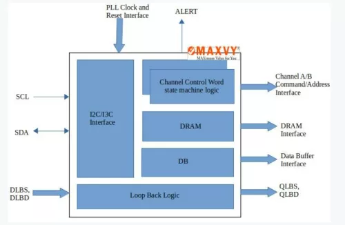
Block Diagram
Applications
- RDIMM
- LRDIMM
- AI (Artificial Intelligence)
- HPC (High-Performance Computing)
- data-intensive applications
Deliverables
- Verilog Source Code
- User Guide
- IP Integration Guide
- Simulation Script
- Synthesis Script
- Encrypted UVM Verification Environment
- cocotb Verification Environment
- Basic Testsuite
Technical Specifications
Maturity
FPGA Proven
Availability
Immediate
Related IPs
- DDR5 Registering Clock Driver (RCD) (DDR5RCD03)
- 622Mbps Laser Driver with Power Control (Vcc=3.3V,Freq=700Mbps, Pulse-Width Distortion=70pS)
- LVPECL Driver
- 100 dB of SNR, 24-bit stereo audio CODEC with headphone driver and digital mixer
- syn1588® enabled IEEE 1588 compliant clock synchronisation
- SMIC18 General process, Multi-Voltage IO, driver current: 10mA~80mA